Electronic Technology Forum
Detailed MOS integrated inverter circuit and input-output characteristic analysis
MOS integrated inverter circuit
Now explain the basis of all circuits-inverters, as an example of the application of MOS integrated circuits. For ease of description, suppose the form of the transistor is a P-channel enhancement type, and the voltage level uses positive logic.
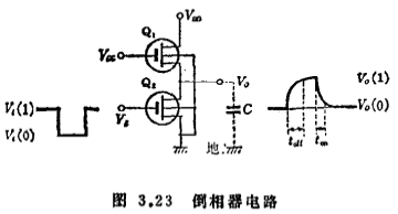
The inverter circuit is composed of two transistors Q1 and Q2 with different transconductance gm in series. Because it is an integrated circuit, the same substrate is used, as shown in Figure 3.23.

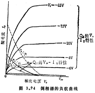
The voltage applied to the gate of the load tube Q1 has the situation of VGG=VDD, and also the situation of |VGG|>|VDD+Vth|. The working state of the former MOS load tube is saturated. Unless otherwise specified, VGG=VDD is the object. MOS integrated inverter circuit. We first consider the basic characteristics. Suppose the drain power supply voltage is VDD (for example, -24V), and when the input voltage gradually increases from zero, the output voltage Vo can be obtained from the operating characteristic curve in Figure 3.24. In Figure 3.24, the output voltage Vo can be obtained from the intersection of the Vo-ID characteristic of Q1 and the Vo-ID characteristic of Q2. For example, the gm of Q2 takes a constant value, and when the gm of Q1 is increased, the output voltage Vo moves in an increasing direction, as shown by the dashed line in Figure 3.24.

At this time, the output voltages Voff and Von can be expressed by the following two formulas respectively.

Where 1/a=L1W2/L2W1,
L1 and L2 are the gate lengths of Q1 and Q2 respectively,
W1 and W2 are the gate widths of Q1 and Q2 respectively,
Vth is the threshold voltage of Q1 and Q2.
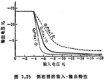
Output voltage: Voff is not equal to VDD, but a level lower than VDD by one Vth. This is unavoidable when MOS transistors are used as load resistors. Therefore, in MOS integrated circuits, the drain voltage should be a voltage higher than the logic swing by Vth. MOS integrated inverter circuit. On the other hand, the output voltage Von is a function of VDD, Vi, Vth, and a, regardless of the absolute value of gm. Figure 3.25 shows the typical characteristics of the output voltage.
Let's consider the switching time of the inverter circuit. In MOS integrated circuits, the input impedance is generally capacitive, and the switching time of the inverter circuit is determined by the charging and discharging time of the load capacitance. Since the movable charge is a majority carrier, the switching time of the MOS transistor itself is very fast and can be ignored. When Q2 is turned on to off, because the charging current from Q1 flows through the load capacitor C, the output voltage gradually increases, and the switching time toff at this time is shown in the following equation.

Where gm1 is Q1![]() ,C is the electrostatic capacitance C1 of the secondary gate, the sum of the source junction capacitance of Q1 and the drain junction capacitance C2 of Q2. Now suppose that the secondary is also connected to an inverter circuit of the same size (the shift register described later is such an example), C1 and C2 are proportional to the gm2 of Q2, so Voffgm2/gm1=L1W2/L2W1=1/a Directly proportional. MOS integrated inverter circuit. On the other hand, from cut-off to turn-on, the charge accumulated on the load capacitor is discharged through Q2. Generally, the gm of Q2 is more than an order of magnitude larger than Q1, and the switching time is extremely fast.
,C is the electrostatic capacitance C1 of the secondary gate, the sum of the source junction capacitance of Q1 and the drain junction capacitance C2 of Q2. Now suppose that the secondary is also connected to an inverter circuit of the same size (the shift register described later is such an example), C1 and C2 are proportional to the gm2 of Q2, so Voffgm2/gm1=L1W2/L2W1=1/a Directly proportional. MOS integrated inverter circuit. On the other hand, from cut-off to turn-on, the charge accumulated on the load capacitor is discharged through Q2. Generally, the gm of Q2 is more than an order of magnitude larger than Q1, and the switching time is extremely fast.

Therefore, the basis of MOS integrated circuits-the input-output characteristics of the inverter circuit-the input-output characteristics and switching characteristics of the phase converter circuit-are only related to the gm ratio of Q1 and Q2, and has nothing to do with the absolute value of gm. Therefore, as long as the gm ratio remains constant, the geometric size of the transistor can be reduced as much as possible within the allowable range of the lithography accuracy.
Contact: Mr. Zou
Contact number: 0755-83888366-8022
Mobile phone: 18123972950
QQ: 2880195519
Contact Address: 5C1, Block CD, Tianji Building, Tianan Digital City, Chegongmiao, Futian District, Shenzhen
Please search WeChat official account: "KIA Semiconductor" or scan the following picture to "Follow" official WeChat official account
Please "follow" the official WeChat account: provide MOS tube technical assistance


