Electronic Technology Forum
Detailed explanation of the key points of MOS integrated circuit design and the determination of geometric dimensions
(1) Consideration of parasitic components
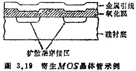
The design of MOS integrated circuits is different from the design of MOS transistors as discrete components. The stray capacitance inside the integrated circuit is small. In order to obtain a certain speed, gm can be made very small, so that the area of the transistor can be made small; at the same time integrated The components of the circuit must be isolated. Key points of MOS integrated circuit design. Regarding the issue of isolation, as shown in Figure 3.19, if the oxide film crosses the two diffusion layer penetration regions and there are metal wiring on the oxide film, it is equivalent to forming a MOS transistor there. The missing part may have the effect of a transistor. Such MOS transistors that appear due to wiring or the like are called parasitic MOS transistors 7).

In order to make the parasitic MOS transistor not work under the bias of the circuit, the oxide layer under the metal wiring is usually thickened to reduce the gm of the transistor. In addition, the threshold voltage of the parasitic transistor should be designed to be higher than the bias voltage as much as possible. This is equivalent to the isolation of bipolar integrated circuits. In the case of complementary type, N-channel transistors are generally isolated.
(2) Determination of material constants
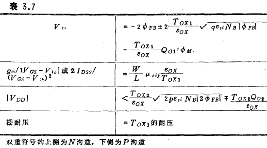
When manufacturing MOS integrated circuits, material constants such as the impurity concentration NB of the semiconductor (currently silicon) substrate, the gate oxide film thickness Tox1, the gate electrode material, and the oxide film thickness Tox2 under the wiring must be determined. Various constant values should meet the conditions of the table when designing. In addition to varying with the impurity concentration of the substrate, μcff in Table 3.7 also varies with the characteristics of the gate oxide film. When SiO2 is used as the oxide film, Qo is positive, and when alumina is used, it is negative. Key points of MOS integrated circuit design. When the substrate impurity concentration is high, it is easy to isolate, but μcff decreases 8), Vth increases above the required value, so the concentration value should be appropriate, usually NB=1015~1016 atoms/cm3, Tox1=1,000~2,000image .png, Tox2=1~1.5μ. SiO2 undergoes high-temperature phosphorus treatment in an atmosphere containing phosphorus pentoxide to stabilize the device. The withstand voltage of the gate oxide film is about 100V, so a parallel reverse-biased P·N junction diode (protection diode) should be connected to the gate connected to the outer lead to prevent insulation damage caused by charging.

(3) Determination of geometric dimensions
In the case of a source-grounded load, the L and W of the amplifying transistor and the load transistor can be of the same order, but in the drain-grounded load transistor, the size ratio determines the gain and output voltage. The gain G of the linear part of the voltage transfer characteristic is
 ,When the input voltage increases, in the over-excitation area
 the output voltage (turn-on voltage) is roughly

When the impurity concentration increases, the voltage gain is smaller than the above simple formula and should be corrected. The size ratio of the amplifying transistor and the load transistor should be selected to meet the requirements of correcting the substrate effect and the required gain and voltage. Key points of MOS integrated circuit design. LA chooses the smallest size that can be achieved by the accuracy of the photolithography technology, and the WA value is selected to achieve the required gm (or drive current) after taking into account factors such as load capacitance. WL can be selected at the same order of magnitude as LA. LL is determined by the size ratio and the other three W and L values.
Contact: Mr. Zou
Contact number: 0755-83888366-8022
Mobile phone: 18123972950
QQ: 2880195519
Contact Address: 5C1, Block CD, Tianji Building, Tianan Digital City, Chegongmiao, Futian District, Shenzhen
Please search WeChat official account: "KIA Semiconductor" or scan the following picture to "Follow" official WeChat official account
Please "follow" the official WeChat account: provide MOS tube technical assistance


