Electronic Technology Forum
Detailed analysis of the functions and process characteristics of MOS integrated circuits
(1) Zoom in
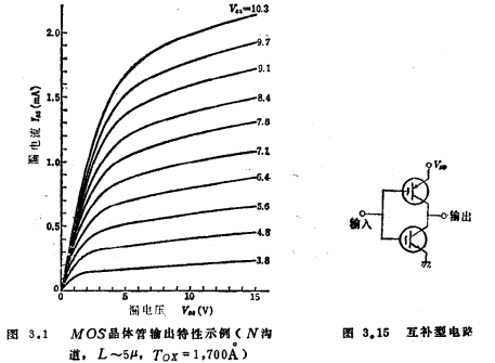
As an active element, the MOS transistor is originally used as an amplifying element. In the complementary circuit shown in Figure 3.15, the P-channel and N-channel transistors work as active components and load components, and are suitable for heavy-load driving and low-power circuits. However, compared with single-channel MOS integrated circuits, the process flow is complicated.

(2) Load
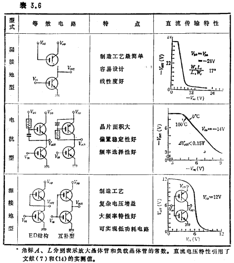
Considering its control parameters and chip area and other individual functions, using MOS transistors as a load is more advantageous than a diffused resistance load. The MOS transistor load utilizes the volt-ampere characteristics between the drain and the source, and is roughly divided into two types according to the form of gate grounding. In the function table 3.65)~7) of MOS integrated circuit, in addition to the two listed above, a reactive load form that has the advantages of both and can realize new functions is added.
The drain ground circuit listed in the table is the most commonly used form at present, and the drain and gate are both AC grounded at this time. In many cases, in order to keep the circuit simple, the drain and the gate are connected together, that is, the DC connection is adopted. This connection is mostly used for enhanced loads. It can be seen from the transmission characteristics that the maximum output voltage must be deducted from the power supply voltage. after the difference is below. In other words, the voltage utilization rate is poor. To overcome this shortcoming, under special circumstances, VG uses another power supply.
On the other hand, the two circuits shown in the source-grounded type column have the characteristic of source-grounded load. In the circuit of the E-D structure, the amplifying transistor is an enhancement type, and the load transistor is a depletion type. Because what is presented is to add Due to the saturation region characteristics of the effective gate bias voltage of a large and small, the load is close to a constant current load. The function of MOS integrated circuit so that the maximum output voltage is almost close to the power supply voltage, and the current charged to the load is also close to constant current, so it has the properties of low power and high speed 8), 9).

Complementary circuit has the same effect as E-D structure, but because the load can be interchanged, it is more beneficial to reduce power consumption. That is to say, no matter the input signal is 1 or 0, there is always one transistor in the off state, and almost no current flows through the two transistors. Only when the image.png is converted, the current that charges the load flows. The reactance type circuit is composed of a leakage grounding circuit and a source grounding circuit. The circuit on the left is drain ground for DC and source ground for AC. The DC transmission characteristics represent this situation. The function of MOS integrated circuit. If the size of the two transistors is roughly the same, the transmission characteristics can be close to 45°, so the DC stability can be improved, and because the source is AC grounded, gain can be obtained. It can also be used for frequency selection. The figure on the left is an example of the same circuit with a complementary configuration.
(3) Transmission gate and analog switch
Since the drain and source can be formed symmetrically for the MOS transistor, the drain and source are the signal terminals of the bidirectional switch, and the gate can be used as the control terminal. However, in bipolar transistors, since a base current as a control signal flows into the signal path, it is difficult to realize a bidirectional function. But for MOS transistors, the bidirectional switch can be used as the transmission gate of the shift register described below, the write and read gate of the memory, etc. Since there is no offset voltage between the drain and the source, it can also be used as an analog switch and a chopper.
(4) Temporary storage
The gate input resistance of the MOS transistor is extremely high, and the time constant determined by the input capacitance and input resistance is usually several milliseconds. Therefore, when a voltage signal is applied to the input terminal and then the signal source is cut off, there will still be leakage current flowing in the millisecond order of time. It can be used to temporarily store information as used in shift registers.
(5) Non-volatile storage
The so-called non-volatile storage is a function that can save the storage contents even after the power is turned off. Since the semiconductor single crystal does not remove the hysteresis after the voltage is applied, it is necessary to use a storage phenomenon that is not a circuit but a physical one. The function of MOS integrated circuit. We believe that if a stable and easy-to-use nonvolatile memory can be made with a simple manufacturing process, the application field of semiconductor memory will be further expanded. Research work in this area is ongoing.
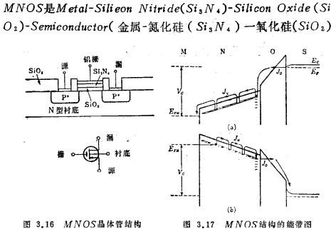
One of these types of memory is to control the surface potential of silicon by using the charges trapped in the traps in the insulating film on silicon. The first non-volatile memory made is an NMOS device, as shown in Figure 3.16. Figure 3.17 is an explanation of the working principle of this kind of device.

Abbreviation for (semiconductor). As shown in Figure 3.17, the difference between the currents flowing through Si3N4 and SiO2 can change the charge charged to the trap at the interface between Si3N4 and SiO2.
When the thickness of SiO2 is about 100~50 time,As shown in Figure 3.17, the current flowing through SiO2 passes through the weak part of the SiO2 barrier due to the tunneling effect. When the thickness of SiO2 is 50
 Below, the direct tunnel current increases.
As this type of non-volatile memory, MAS transistors 10) using Al2O3 as insulators and MAOS transistors 11) using Al2O3~SiO2 as insulators have been published.

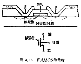
There is also a non-volatile memory that does not use the tunneling phenomenon of the charge passing through the insulator, but uses the phenomenon that the high-energy charge generated by the avalanche breakdown of the PN junction crosses the insulator barrier. The function of MOS integrated circuit. Figure 3.1812) is a non-volatile memory using a floating gate. The electrons generated by avalanche breakdown of the drain junction are injected over SiO2 into the floating gate made of polysilicon. Once the electrons are injected, they are surrounded by highly insulating SiO2, so Can be stored for a long time. Regarding this method of using avalanche breakdown, there is also the use of injected electrons for writing, and in the same way, the electrically rewritable memory 13) which is erased by injected holes.
This kind of memory readout, in most cases, uses the MOS transistor structure shown in Figure 3.16 and Figure 3.18 to measure the current between the source and the drain caused by the surface potential change.
Contact: Mr. Zou
Contact number: 0755-83888366-8022
Mobile phone: 18123972950
QQ: 2880195519
Contact Address: 5C1, Block CD, Tianji Building, Tianan Digital City, Chegongmiao, Futian District, Shenzhen
Please search WeChat official account: "KIA Semiconductor" or scan the following picture to "Follow" official WeChat official account
Please "follow" the official WeChat account: provide MOS tube technical assistance


