Electronic Technology Forum
Detailed explanation of the four classification characteristics and working principles of MOS integrated flip-flop circuits
In various control instruments and desktop electronic computers and other equipment, various MOS integrated circuit trigger circuits are used, and they can be divided into four categories.
(1) R-S flip-flop circuit and R-S-S flip-flop circuit
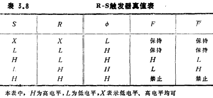
The truth table of the R-S flip-flop circuit is shown in Table 3.8. When the set (S) and reset (R) are both "L" and the clock (ф) is also "L", the output is in the hold state; when the clock ф is "H", the S and R inputs are valid, and ф Synchronous changes. But when S and R are both H, the output state cannot be uniquely determined, so it is in the "prohibited" state.
The circuit for logic operation according to this truth table is shown in Figure 3.32. The flip-flop circuit consists of Q4 and Q5, which are transmitted through their respective output inverters Q9 and Q10. Q1, Q2 and Q7, Q8 respectively constitute an "AND" gate.
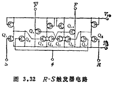
Let's explain how it works.
When the level of ф is I, Q2 and Q7 are in the conducting state, so no matter what the level of S and R, the signal can not be sent in, and the state of the flip-flop circuit remains unchanged. When the S and R levels are in the L state, the same state appears.
However, when the level of ф changes to H and S=H, R=L, Q3 is turned on, and its output terminal is connected to the gate of Q5 to turn off Q5, so the inverted output signal HL appears in  two end. When S=L and R=H, the same action is generated for Q6 and Q4 of the flip-flop circuit, and the output of F=L,
  is obtained. When S=R=H, Q3 and Q6 are both on, and
  is all L. In this state, the flip-flop does not work and is a prohibited state.
The operation of this flip-flop circuit is as described above. But if you pay attention to the clock signal, when the clock flips from L to H, the output changes, as shown in the time chart shown in Figure 3.33.
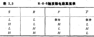
Let's study the R-S-S flip-flop circuit. The basic working principle of this circuit is the same as that of the R-S flip-flop circuit, but in the forbidden state of S=R=H, it must be set first, that is, it becomes a circuit that performs S=H, R=L work. Therefore, its truth table is shown in Table 3.9.
The circuit diagram is shown in Figure 3.34. Q6, Q7, and Q8 form the flip-flop circuit, and the input signal from the gate circuit composed of Q2, Q3, and Q4 enters the circuit through the clock control gate Q5. The output signal of the flip-flop appears at the output terminal through the clock control gates of Q9 and Q12 and the buffer circuits of Q10, Q11 and Q13, Q14. When S=R=L, if the input signal of Q4 is L, both Q3 and Q4 are turned on, leading to the output signal of Q2 generated by the S signal, and the input signal of Q5 becomes H. In this state, if ф1 is L, then Q5 is turned on, the gate of Q6 becomes H, and the gate of Q7 becomes L. This state is maintained by the gate capacitance of Q6 after ф1 is turned to H (holding time is 100 microseconds). Then if ф2 becomes L, Q9 and Q12 are turned on, and the output signal of Q6 and Q7 are transmitted to Q10 and Q13 respectively. The output signal of Q7 can also be added to the gate of Q6 through Q8 to supplement the discharge loss of the charge accumulated on the gate capacitance of Q6.
In addition, when the input signal of Q4 is H, Q4 is cut off, so S=L directly becomes the input signal of the trigger, H appears on  , and L appears on Q. That is, the output state remains unchanged. When S=H and R=L, the output signal of Q2 is H, regardless of the state of
  , it becomes
  =L, Q=H. When S=L and R=H, Q2, Q2, and Q4 are in the cut-off state. Contrary to the above situation,
  =H, Q=L. When S=R=H, because R=H, Q3 ends, regardless of the state of
  , it becomes S leading, and
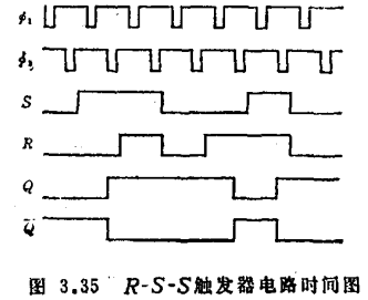
  =L, Q=H. This circuit is different from the aforementioned R-S flip-flop circuit. The clock has two phases of ф1 and ф2. ф1 is used to write the signal and ф2 is used to read the signal. So there is the time chart in Figure 3.35. MOS integrated circuits have the advantage of simplifying circuits by using multiphase clocks. Two-phase triggers have been sold.
(2) J-K flip-flop circuit
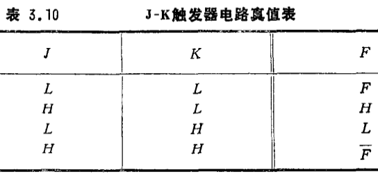
This circuit is basically the same as the R-S flip-flop, which is a flip-flop with a flip function when J=K=H. The truth table is shown in Table 3.10.
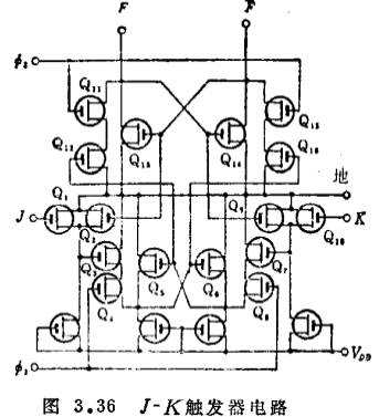
The equivalent circuit is shown in Figure 3.36. The master flip-flop composed of Q5 and Q6 and the slave flip-flop composed of Q13 and Q14 form a J-K flip-flop. When ф 1 is L, Q4 and Q8 are turned on, and the input signals of J and K are placed in the main flip-flops Q5 and Q6 through the gate circuits of Q3 and Q7. Then when the ф2 clock turns to L, the output signals of Q5 and Q6 enter Q12 and Q16, so the flip-flops Q13 and Q14 are set, and the synchronization signal is output from  . When J=K=L, Q3 and Q7 are cut off, even if ф1 becomes L, the signal does not enter the main flip-flop, and the state of the flip-flop remains unchanged. When J=H, K=L, Q=H,
 , and the feedback signals of
  and
and  make Q3 cut off. Since K=L, Q7 is also cut off, so the state of the main flip-flop remains unchanged. Conversely, when
  =L and
  =H, Q7 is turned off, and the input signal of J turns off Q1, and Q2 is also turned off due to the feedback signal, so Q3 is turned on. In this state, if ф1 changes to L, the main flip-flop is placed in a state where Q6 is off and Q5 is on. If then ф2 becomes L, the signal enters the slave flip-flop, and the output becomes Q=H,
  =L, as in the above case, when J=
When H, K=I, it has nothing to do with the previous state of  , Q=H,
  =L. In addition, when the input is J=L, K=H, because the circuit is symmetrical, it is completely opposite to the situation of J=H, K=L, and the output is set to the state of Q=L,
  =H. When J=K=H, in the state of Q=H,
  =L, Q3 is off and Q7 is on, so with the help of the clock of ф 1=L, the main flip-flop and input are J=L, K= In the case of H, it is set in the same way. After adding the clock of ф 2=L, Q=L,
  , and the output signal is reversed.
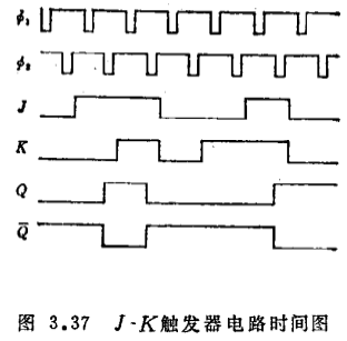
It can be seen from the work of the J-K flip-flop above that the clock is two-phase, and ф1 and ф2 are added to make the flip-flop work. The signal is written in the previous clock and the signal is read out in the latter clock. The time chart is shown in Figure 3.37.
(3) Binary flip-flop circuit
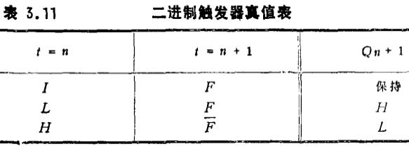
This kind of circuit is a flip-flop circuit that corresponds to one cycle of the input signal and the output flips once. In the circuit of Figure 3.38, the output is reversed when the input changes from H to L. The truth table is shown in Table 3.11.
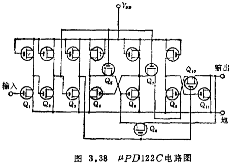
In Figure 3.38, Q4, Q5, and Q6 constitute the master flip-flop, Q9, Q10, and Q11 constitute the slave flip-flop, Q7 is the gate that transmits signals from the master flip-flop to the slave flip-flop, and Q8 is the gate from the slave flip-flop to the master flip-flop Signal transmission gate. Now consider the situation where the output is in the H state and the input changes from H to L. When the input is H, the transmission gate Q7 is turned off, Q8 is turned on, the output signal returns to the main flip-flop, Q6 is turned off, and Q4 is turned on. Then if the input becomes L, the transmission gate Q7 is turned on and Q8 is turned off, so the level of Q6 is transmitted to Q9 through Q7, and Q9 is turned on, so Q11 is turned off, and the output is reversed. When the input returns to H again, Q7 is off and Q8 is on. As long as the state of the flip-flop is transferred to the main flip-flop, the output state remains unchanged.
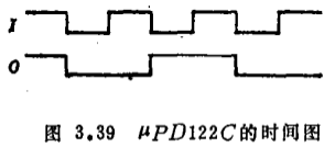
In short, when the input is H, regardless of the output state, the flip-flop state can be maintained; when the input changes from H to L, the flip-flop flips, so the truth table is shown in Table 3.11, and the timing diagram is shown in Figure 3.39 .
Contact: Mr. Zou
Contact number: 0755-83888366-8022
Mobile phone: 18123972950
QQ: 2880195519
Contact Address: 5C1, Block CD, Tianji Building, Tianan Digital City, Chegongmiao, Futian District, Shenzhen
Please search WeChat official account: "KIA Semiconductor" or scan the following picture to "Follow" official WeChat official account
Please "follow" the official WeChat account: provide MOS tube technical assistance


