Electronic Technology Forum
Layout of MOS integrated gate circuit-Analysis of characteristics of input/output and switch circuit
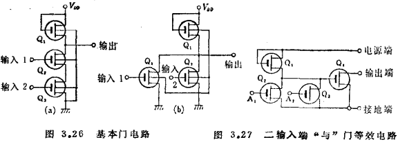
The gate circuit can be considered as a variation of the inverter circuit, basically there are series and parallel modes shown in Figure 3.26. The circuit in Figure (a) is a two-input NOR gate (positive logic) or a NAND gate (negative logic). Generally, in this circuit mode, the output voltage depends on the sum of the on-resistances of the two drive tubes Q2 and Q3. In order to obtain the same characteristics as the circuit in Figure (b), the area of the transistor must be increased and its transconductance gm must be increased. This is very uneconomical. So there are few examples.

The circuit in Figure (b) is a two-input NAND gate (positive logic) or a NOR gate (negative logic). MOS integrated gate circuit. The load of this gate circuit is the gate of the secondary MOS transistor connected to it. In order to shorten the switching time, as described in the inverter circuit in section 3.3.1, the gm of Q1 must be increased. Von only depends on the gm of Q1 and Q2, so the area of Q2 must also increase. As a result, it becomes uneconomical to increase the area of the transistor under the premise of ensuring the necessary number of input terminals. MOS integrated gate circuit. Therefore, a first-stage inverter circuit is generally added to the output terminal of the gate circuit. The equivalent circuit is shown in Figure 3.27. Figure 3.28 shows the plane layout of this circuit after it is made into an integrated circuit.
The black bars on the figure indicate the gate area, Q1 has an L of 15μ, and Q2~Q4 has an L of 10μ. Q1 is a load MOS transistor, and its W is 15μ, while Q2 and Q3 are drive MOS transistors, and its W is 280μ. Q4 wants to drive the large load capacitance connected to the output stage, gm must be very large, so the W of the tube must be increased to 735μ. It can be seen from Figure 3.28 that the boron diffusion area, aluminum wiring portion, and gate oxide film that constitute the source and drain regions are properly laid out to minimize the area of the entire pattern.

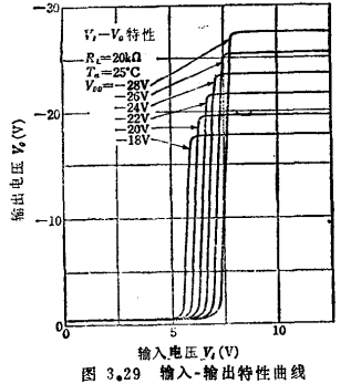
The typical input-output characteristics of the above gate circuit are shown in Figure 3.29.

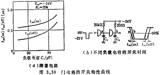
This figure gives the load resistance as ,The parameter VDD changes in the range of -28~-18V. The switching time is measured with the circuit shown in Figure 3.30(a). MOS integrated gate circuit. As mentioned earlier, the switching time of the MOS circuit varies with the load capacitance. An example of the characteristic curve is shown in Figure 3.30(b).

Utilizing the bidirectional characteristic of MOS transistors, the gate circuit for analog switch circuits as shown in Figure 3.31 can be made.

The input signal is added to G1, G2,...G6, assuming that the source S1...S6 is a signal source, then a signal appears at the output terminal D. If a voltage close to the source voltage is applied to the gate, the transistor can be turned off. Because the cut-off characteristics of the MOS transistor are extremely good, the S/N ratio can be achieved very high.
Contact: Mr. Zou
Contact number: 0755-83888366-8022
Mobile phone: 18123972950
QQ: 2880195519
Contact Address: 5C1, Block CD, Tianji Building, Tianan Digital City, Chegongmiao, Futian District, Shenzhen
Please search WeChat official account: "KIA Semiconductor" or scan the following picture to "Follow" official WeChat official account
Please "follow" the official WeChat account: provide MOS tube technical assistance


