MOS J-K tube flip-flop, J-K tube flip-flop working principle, J-K tube design considerations, J-K flip-flop also includes a master flip-flop and a slave flip-flop, but it is different from the genera
MOS J-K tube flip-flop, J-K tube flip-flop working principle, J-K tube design considerations, J-K flip-flop also includes a master flip-flop and a slave flip-flop, but it is different from the genera

MOS R Logic gates such as "NOT" gate, "NAND", "NOR" and "AND NOR". The output of these logic gates is determined by the input state. If the input state changes, the output changes accordingly. Logic
MOS R Logic gates such as "NOT" gate, "NAND", "NOR" and "AND NOR". The output of these logic gates is determined by the input state. If the input state changes, the output changes accordingly. Logic

MOS transmission gate MOS transistors have a very useful feature-bidirectionality. Because its source and drain are exactly the same, they can exchange work with each other. When a gate voltage exc
MOS transmission gate MOS transistors have a very useful feature-bidirectionality. Because its source and drain are exactly the same, they can exchange work with each other. When a gate voltage exc
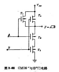
CMOS gate circuit (NAND gate, NOR gate, OD gate, transmission gate, tri-state gate) is introduced in detail. Figure 2-68 shows the CMOS NAND gate circuit, where image.png is two NMOS in series The ima
CMOS gate circuit (NAND gate, NOR gate, OD gate, transmission gate, tri-state gate) is introduced in detail. Figure 2-68 shows the CMOS NAND gate circuit, where image.png is two NMOS in series The ima
Detailed explanation and general analysis of single-channel MOS gate circuit, single-channel MOS gate circuit, the various inverters described above, is a "not" gate circuit, which has the function of
Detailed explanation and general analysis of single-channel MOS gate circuit, single-channel MOS gate circuit, the various inverters described above, is a "not" gate circuit, which has the function of
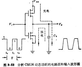
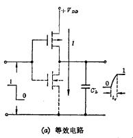
CMOS inverter power consumption discussion and analysis in detail, CMOS inverter power consumption discussion, CMOS circuit static power consumption is very low, can be ignored. The power consumption
CMOS inverter power consumption discussion and analysis in detail, CMOS inverter power consumption discussion, CMOS circuit static power consumption is very low, can be ignored. The power consumption
The transient response of the CMOS inverter, from the analysis of the transient characteristics of the single-channel MOS inverter, we know that the frequency response of the MOS tube itself that comp
The transient response of the CMOS inverter, from the analysis of the transient characteristics of the single-channel MOS inverter, we know that the frequency response of the MOS tube itself that comp
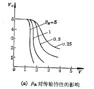
Transmission characteristics of CMOS inverters 1. DC transmission characteristics and noise tolerance, CMOS transmission characteristics, as everyone knows, the transmission characteristic curve of th
Transmission characteristics of CMOS inverters 1. DC transmission characteristics and noise tolerance, CMOS transmission characteristics, as everyone knows, the transmission characteristic curve of th
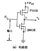
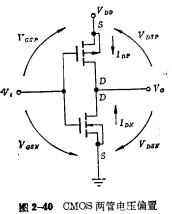
The CMOS inverter is composed of an enhanced P-channel MOS tube and an enhanced N-channel MOS tube. The NMOS tube is used as the input tube and the PMOS tube is used as the load tube.
The CMOS inverter is composed of an enhanced P-channel MOS tube and an enhanced N-channel MOS tube. The NMOS tube is used as the input tube and the PMOS tube is used as the load tube.
E/DMOS inverter static analysis and detailed explanation 1. Output voltage discussion, two operating points on the output characteristic curve of the inverter, point A (on) corresponds to the output l
E/DMOS inverter static analysis and detailed explanation 1. Output voltage discussion, two operating points on the output characteristic curve of the inverter, point A (on) corresponds to the output l


5C1, CD Block, Tianji Building, Tianan Digital City, Futian District, Shenzhen

KIA-The Public