Electronic Technology Forum
CMOS inverter power consumption discussion and analysis in detail
CMOS inverter power consumptiondiscussion
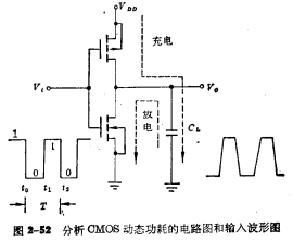
The static power consumption of the CMOS circuit is very low and can be ignored. The power consumption to be discussed here is mainly due to the dynamic power consumption consumed by charging and discharging the load capacitor during the switching process. Now make two assumptions:
①The input signal is a step wave. Under this assumption, the input tube and load tube will not be turned on at the same time.
②The repetition frequency of the input signal is far less than the maximum operating frequency of the inverter. The voltage on the load capacitor  at the end of the inverter conversion process It can reach a stable low level 0V or high level VDD. CMOS inverter power consumption discussion
In the process of charging and discharging the load capacitance of the inverter, only the load capacitance only consumes power supply current when charging, and the load capacitor
  When discharging through the input tube, because the load tube is cut off, there is no DC path from the power supply to the ground, so the power supply current is not consumed.
It can be seen from the input waveform in Figure 2-52 that in one cycle , the load tube is turned on only when the input is low level, and the load capacitance is
  Charging consumes power supply current. CMOS inverter power consumption discussion, during this period of time, the energy consumed by the power supply is equal to one cycle
 . The specific calculation is as follows:

The energy consumed in dt time is:

Because of 
hem d so change the (2-89) formula to:

To (2-90) integral, in  During this time, the voltage across the capacitor is charged from 0 to VDD, so it will disappear during this time. span style="font-size: 18px;">The total energy consumed is:

Average power consumption per cycle:
f is the repetition frequency of the input pulse.
This formula indicates that when the input is a step wave, the dynamic power consumption is only related to the load capacitance, operating frequency, and power supply voltage, and has nothing to do with the parameters of the device.
In actual work, the input is not a step wave, so it will cause significant rise and fall time delays. Therefore, both MOS transistors are partially turned on at the moment of level conversion. CMOS inverter power consumption discussion, during device switching, not all current is used to charge and discharge the capacitor, and there is a direct path from the power supply to the ground, so additional power consumption is caused. . In addition, there is static power consumption
  , so the total MOS inverter Power consumption is:
 < br/>
 is The total DC leakage current, including the cut-off current of the MOS tube and the reverse leakage current of the parasitic diode, is related to the size of the devices that make up the circuit, the number of gates, and the level of technology. When the temperature rises, this kind of leakage becomes more obvious. .
Example: Consider a 50-door matrix,  , the repetition frequency of the input signal is
  , total load capacitance O
 , Find the total power consumption.
 < br/>
If a bipolar 50 gate matrix is used, the power consumption is one hundred times that of CMOS and 10 times that of PMOS. It can be seen that CMOS has the least power consumption.
In a high-speed circuit system, most of the power consumption is dynamic power consumption, while static power consumption is negligible. But when the operating frequency is very low, the static power consumption cannot be ignored compared with the dynamic power consumption.
In fact, the inverter power consumption can be approximately expressed as:

Among them is to measure the total current of the DC power supply.
Contact: Mr. Zou
Tel: 0755-83888366-8022
Mobile: 18123972950
QQ: 2880195519
Address: 5C1, CD Block, Tianji Building, Tian’an Digital City, Chegongmiao, Futian District, Shenzhen
Please search WeChat Official Account: "KIA Semiconductor" or scan the following picture to "Follow" Official WeChat Official Account
Please "follow" the official WeChat account: provide MOS tube technical assistance


