Electronic Technology Forum
Detailed explanation and general analysis of single-channel MOS gate circuit
1. Single channel MOS gate circuit
The various inverters described above are just a "not" gate circuit with a logical "not" function. That is, the input is "1" and the output is "0"; otherwise, the input is "0" and the output is "1".
MOS gates, single-channel MOS gates can be divided into single-channel gates and double-channel gates according to the similarities and differences between the input device and the channel of the load device. The load and input devices of the E/EMOS and E/DMOS inverters mentioned above are composed of the same channel, which is a single channel circuit; while the channel of the load tube and the input tube of the CMOS circuit are different , It is a dual-channel circuit. Below we respectively introduce some basic forms of MOS gate circuits. In the discussion, unless otherwise specified, they are all prescribed by positive logic.
1, "NAND" gate circuit
Figure 2-53 shows the E/EMOS NAND gate circuit and E/DMOS NAND gate circuit. Figure 2-53 (a) is composed of three N-channel enhanced MOS transistors,  The input tube is connected in series, and
  is the load tube. Figure 2-53(b) consists of two enhanced tubes and a depleted tube,
 The serial connection is the input tube,
 is the load tube. A and B are the input terminals, and F is the output terminal.
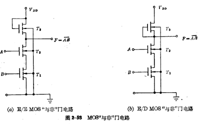
When the two input terminals A and B are at the same time Turn on, because the on-resistance is very small, so the output is "0" level. When either of the two input terminals A and B is "0", that is,
  or
or  The tube is off, and the entire circuit cannot be turned on. The output is "1" level. Obviously, the relationship between output F and inputs A and B is NAND. The logical formula is
  .
.
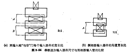
The form of the NAND gate circuit is the same as that of the inverter circuit, the difference is that several series-connected input tubes replace one of the inverter Enter the tube. If the channel width-to-length ratio of each input tube in series is equal to that of the inverter, then the NAND gate circuit at the two input ends should have an equivalent conduction resistance equal to 2 of the on-resistance of the input tube of the inverter. Times. For a single-channel MOS gate circuit, when the two input tubes of the NAND gate are all turned on, the output low level is equal to twice that of the inverter, which is undesirable. In order to achieve the same value as the inverter output low level, the equivalent resistance of each input tube connected in series must be half that of the inverter during the design, that is, the channel width to length ratio must be equal to the inverted 2 times the phaser. If there are NAND gate circuits with N input terminals, obviously the channel width-to-length ratio of each input tube should be equal to N times of the input tube of the inverter.

Figure 2-54 shows that the area of the geometrical figure of the series superimposed device is many times larger than the area occupied by the input tube of the inverter, so the circuit pattern occupies a large crystal surface , Affect the integration level and process yield. In addition, the parasitic capacitance increases, which has a negative impact on the switching speed. In addition, when the series selection is added, the source potential of the A input device above is higher than the source potential (ground potential) of the B device. When the 4 and B input are the same At the "1" level, (Va)4*(Vos), therefore, to make the on-resistance of the A device equal to that of the B device, it is required to 
Taking into account the above reasons, avoid the use of superposition as much as possible in the logic design of MOS circuits. At the same time, a practical limit is also put forward for the number of series-connected devices, because as the number of series-connected devices increases, the above-mentioned influence will become more serious. Therefore, no more than three devices in series are usually appropriate.
2, "NOR" gate circuit
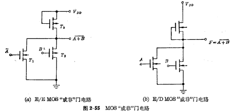
Figure 2-55 shows the NOR gate circuit with two input terminals. Among them 2-55 (a) is E/E MOS"NOR" gate circuit, composed of 3 N-channel enhanced MOS transistors ,  and
and  The input tube is connected in parallel; Figure 2-55(b) is the E/D MOS "NOR" gate circuit,
  is an N-channel enhanced MOS tube,
  is an N-channel depletion MOS transistor.
When  input is "0",
  until the end, the output is "1" level; when
  or
or  , enter "1" for any tube,
 or
or  As long as one tube is turned on, the output will be "0" level. So the output
  and input A and B are "or not".
The logical formula is: 
In the NOR gate circuit, the size of each input tube should be the same as that of the inverter. Because as long as any branch of the parallel device is in the conducting state, its conduction equivalent resistance is the same as that of the inverter input device. If several parallel devices are conducting at the same time, the output low level will be lower. . Figure 2-56 shows that the width-to-length ratio of a single device channel of a parallel gate is the same as that of the inverter input device.
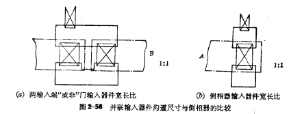
For the NOR gates with parallel input tubes, since the width-to-length ratio of the device should not be increased, it is superior to the input tubes in series in terms of improving integration, reducing parasitic capacitance, and expanding the number of input terminals. Therefore, in the design of MOS logic circuits, input tubes are generally connected in parallel. Figure 2-56 shows that the width-to-length ratio of a single device channel of a parallel gate is the same as that of the inverter input device. , For some NAND gates that need to increase the number of input terminals, in order to avoid the disadvantages of series work, they are often connected in parallel.
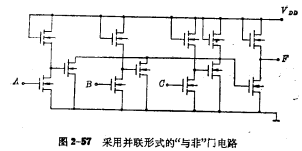
Figure 2-57 shows the three-input "NAND" gate circuit formed in parallel. The logical formula can be obtained by inversion, namely:

Because this method increases the number of gate stages, the transmission delay time is somewhat increased.
3, "AND" gate, "OR" gate and "AND NOR" gate circuit
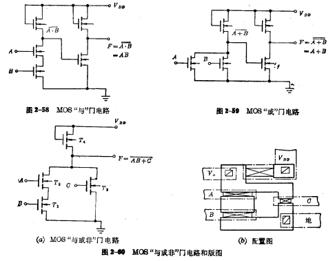
Add an inverter behind the above-mentioned "NAND" gate to form a "AND" circuit, as shown in Figure 2-58. Similarly, add an inverter behind the NOR gate to form an OR gate circuit, as shown in Figure 2-59. If there are three input devices Apply for the Union, and
  Parallel, the gate circuit formed in this way is < span>AND NOR gate circuit; if an inverter is added at the back, it becomes an AND OR gate circuit, as shown in Figure 2-60.
From Figure 2-60(b), it can be seen that the aspect ratio of the two series-connected devices is twice that of the parallel-connected devices.
4, "exclusive OR" gate circuit
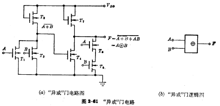
Figure 2-61 (a) and (b) are the "exclusive OR" circuit and its logic symbols, respectively, where  and
and  Form a first-level "NOR" gate,
 ; forms the second level "AND NOR gate,
 The input of is the output of the first-level NOR gate. The relationship between input and output is:

Its logic function can be described as follows: If A and B input the same "1" level or "0" level, the output is "0" Otherwise, if the A and B inputs are different, the output will be at "1" level.
There is also a relatively simple circuit of the "exclusive OR" gate, as shown in Figure 2-62, where  is the gate control,
  is Load tube,
  constitutes an inverter.
The working principle is this: when A and B are both "1" or both are "0", the gate-source voltage Vos of "1" and "T" Both are 0V and cannot be turned on. The output at point F'is "1" level. After phase inversion, the output terminal F is "0" level; if the levels of A and B are different, for example, A is "1", B Is "0", then  ends,
ends,  Turn on, F' point output is "0" level , Through phase inversion, the output terminal F is "1". The function of the "exclusive OR" gate is completed.
If a level of NOT gate is added behind the “exclusive OR” gate, it will constitute an “exclusive OR ” gate, and its logical formula is:

The "exclusive NOR" gate is also called the "identical OR" gate. Its logic function can be described as follows: when the A and B input terminals are the same, the output is "1" when the A and B input terminals are different, the output is "0".
In E/DMOS circuits, it can also be composed of "OR" gates, "AND" gates, "XOR", "XOR" gates in the same form as E/EMOS Circuit. I will not elaborate here, please refer to the relevant information for readers.
5. Drive circuit
The input terminal of MOS integrated circuit is generally the gate of MOS tube, so no matter the input is "0"
level or "1" level, no current flows into the circuit, and no current flows out of the circuit. If a drive circuit is used to drive another circuit; whether it is outputting a "0" level or a "1" level, neither the current of the driven circuit flows into the drive circuit nor the current of the drive circuit flows into it. Driven circuit. This is completely different from TTL circuits. In this way, can one MOS circuit drive any number of MOS gate circuits? That is, can its load capacity be infinite?
Of course not, because speed must also be considered.
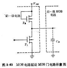
As you all know, the input terminal of every MOS integrated circuit has a certain capacitance to ground. If many MOS gate circuits connected in parallel are driven, the The input capacitance must be added together to become a large load capacitance of the output stage, as shown in Figure 2-63. Therefore, when the input level of the output stage changes from "1" to "0", T1 changes from on to off, and the input capacitance of the driven circuit  It is necessary to charge through the load tube of the previous stage. If there are many gates to be driven, input capacitance
 is very big, the cut-off time of the previous level is very long, the speed will be reduced, so in order to ensure that the circuit has For a certain switching speed, the load capacity of the circuit is bound to be limited.
In order to improve the load capacity of the MOS integrated circuit, it is necessary to increase the driving ability, but also to reduce the load tube without increasing the cut-off time. on-resistance (that is, increase
  aspect ratio). When discussing the E/E saturated load MOS inverter, it has been pointed out that in order to achieve a lower low-level output, the width-to-length ratio of the load tube (W/L) and the width-to-length ratio of the input tube (W/L)< span style="font-size: 10px;">L, should maintain a certain ratio. Therefore, to increase the aspect ratio (W/L) z of the load tube, the aspect ratio of the input tube must be increased accordingly
 , in this way, not only greatly increases the footprint of the chip, but also increases the parasitic capacitance, which increases the load capacitance of the previous stage. Therefore, this method is not advisable.
In order to improve the load capacity of MOS integrated circuits, people use the MOS output stage circuit shown in Figure 2-64, which consists of four MOS tubes, of which  forms a saturated load MOS inverter,
  The aspect ratio of the two tubes is larger. The following figure 2-64 (a) to illustrate its working principle. When the input terminal
  is "0" level,
  The deadline is so that
  The tube is turned on, and the output level is "1". Under static conditions,
  and
and  There is always one cut-off, so the static power consumption of this pair of tubes is zero. Therefore, regardless of the W/L of
  and
and  What is the W/L ratio, and the output "0" level is all zero. Single channel MOS gate circuit. So you can use
  and
and  The W/L is the same, and the larger value is used. When the output level changes from "0" to "1", the load capacitance
  can be charged via
  When the output level changes from "1" to "0", the load capacitance
  You can use
  Discharge. Such as
  and
and  If the W/L is larger and the same, the charging and discharging time of the load capacitor will be very short. Therefore, this kind of electrical network can drive a larger load capacitance at a faster speed. Because of
  and
and  Works in turn under pulse conditions, so it is called an inverting push-pull output stage.
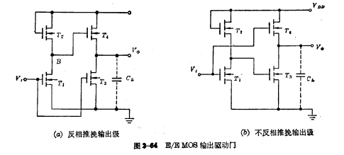
If you want to make the output stage non-inverting, you can change the circuit structure to the form shown in Figure 2-64(b). Its working principle is exactly the same as the inverting push-pull output stage.
Although the above-mentioned output stage circuit can increase the driving capacity, and the output "0" level is close to 0V, it outputs "1" level with a small value . For the circuit in Figure 2-64(a), when input  When the level is "0",
  ends,
ends,  The grid voltage of is
  . Because
  The gate source voltage is greater than
  can be turned on, so the output "1" level should be
  In order to increase the value of the output high level, the above circuit can be improved. One method is in the circuit of Figure 2-64(a)
  Connect a small transconductance
  tube in parallel (Figure 2 -65), the width to length ratio of this tube can be made smaller than the saturated load tube. In this way, relying on
  to provide a larger charging current, relying on
  Increase the value of the output high level.
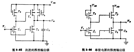
In addition, the structure of connecting two sets of power supplies can be adopted, as shown in Figure 2-66. If you use  , output "1" level can reach
  .
.
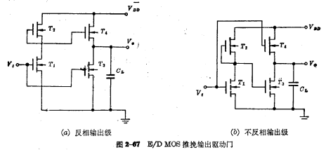
For E/DMOS circuits, there are also push-pull output stage circuits in the same form (as shown in Figure 2-67), where (a) is the inverted output circuit, (b ) Is the in-phase output circuit. Its working principle is similar to the above-mentioned E/EMOS output stage circuit, and readers can analyze it by themselves.
Contact: Mr. Zou
Tel: 0755-83888366-8022
Mobile: 18123972950
QQ: 2880195519
Contact address: 5C1, CD Block, Tianji Building, Tian’an Digital City, Chegongmiao, Futian District, Shenzhen
Please search the WeChat official account: "KIA Semiconductor" or scan the picture below to "Follow" the official WeChat official account
Please "follow" the official WeChat account: provide MOS tube technical assistance


