Electronic Technology Forum
Detailed explanation of the working principle of MOS transmission gate and single channel transmission gate (high level and low level)
MOS transistors have a very useful feature-bidirectionality. Because its source and drain are exactly the same, they can exchange work with each other. When a grid voltage exceeding the threshold voltage  is applied to the grid As the voltage polarity between the source and drain is different, the current can flow from the left to the right, or from the right to the left. If the current flows from left to right, it is considered that the pole on the left is D and the pole on the right is S. On the contrary, the right side is the D pole and the left side is the S pole. Using the above characteristics, it can be miniaturized into a kind of electronic switch, that is, the so-called transmission gate, which can be divided into a single-channel transmission gate and a double-channel (CMOS) transmission gate according to different channel conditions. Here is how they work.
1, single channel transmission gate
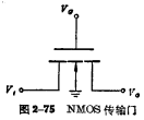
Figure 2-75 shows the NMOS single-channel transmission gate. Its gate is connected to the control voltage, the substrate is grounded, and the input and output terminals can be selected arbitrarily. The left side of the figure is set as the input terminal, and the right side is set as the output terminal. The transmission gate can set high level "1" and low level< span>"0" is passed from the input to the output. The cases of transmitting "1" and transmitting "0" are discussed below.

(1) High-level transmission
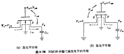
Figure 2-76(a) is a schematic diagram of high-level transmission. Assuming the original grid voltage  , input voltage
  , output terminal
 (i.e. the grid and output voltage
  ), which is greater than the threshold voltage of the tube
 , the transmission gate is opened, input voltage
  , through the conductive pair capacitor
  Charge. It can be seen that the current flows from to the right, so the left side is defined as the drain and the right side is defined as the source. With
  voltage across both ends
 The increase in gate-source voltage
 As it becomes smaller, the channel resistance of the gate increases, the conduction condition becomes worse, and the charging current becomes smaller and smaller,
  The rising speed is getting slower and slower. When the capacitor
  is charged to
  , at this time
 approaches 0, and the transmission gate is critically closed. Therefore, the maximum output voltage of the transmission gate can only reach
 , even if the input voltage is increased
 , it will not make
  Increase, if the input voltage is to be transmitted to the output terminal, the control voltage must be increased to make
  , this will increase the complexity of the circuit.

As mentioned above, when the single-channel transmission gate transmits a high level, there is a premature cut-off situation, which limits the amplitude of the transmission voltage and the channel resistance The changes are large and limit the switching speed.
(2) Low-level transmission
Figure 2-76(b) is a schematic diagram of low-level transmission. Assuming that the original is closed, that is: 
 . When the control voltage
  is applied to the gate, the transmission gate is opened and the capacitance
  It discharges through the turned-on gate, and the current flows from the output to the input Therefore, the right side is defined as the drain of the pipe, and the left side is defined as the source of the pipe. Since the input terminal is always 0, the gate-source voltage
  is also constant< img src="/userfiles/images/2020/11/10/2020111010539672.png" title="image.png" alt="image.png"/> Therefore, the tube is always turned on during the transmission process, and the output terminal voltage It can reach the same amplitude as the input voltage. In addition, the capacitor
  must pass through the saturation zone of the tube during discharge And the unsaturated zone. Since the voltage at both ends of
  decreases with time, the discharge speed is The slower it comes, which limits the switching speed of the circuit.
2, CMOS transmission gate
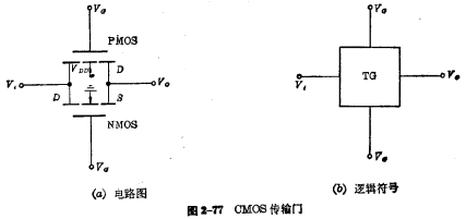
The CMOS transmission gate is made up of a PMOS tube and an NMOS tube in parallel. As shown in Figure 2-77. It has better transmission characteristics than a single-channel transmission gate, and the transmission voltage can be any value from 0 to the power supply voltage.

This is a pair of complementary MOS transistors, the source and drain are connected to each other to form the input and output ends; the substrate of the PMOS tube is connected to the power supply , the substrate ground potential of the NMOS tube; the gates of the two tubes are respectively connected to the complementary control voltage VG and VG , When one is at high level, the other is at low level.
When ,
,  When both tubes are on, the transmission gate is on Status, the signal from the input terminal can be transmitted to the output terminal; when
  , Both tubes are cut off, the transmission gate is cut off, and the signal at the input end cannot be transmitted to the output end.
The following will discuss the high-level transmission and low-level transmission respectively.
(1) High level transmission
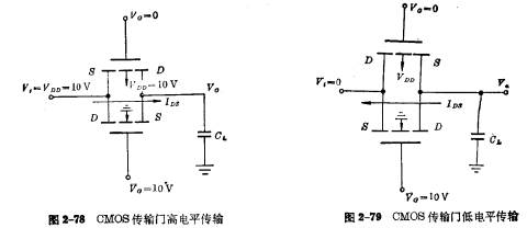
Figure 2-78 shows the actual circuit of high-level transmission. Set the input voltage  , the original
  . When adding the control signal
  ,
, , NMOS tube
 , both tubes are fully turned on, and the transmission door is opened. At this time, the input voltage charges the capacitor
  through the turned-on complementary tube . According to the direction of current flow, the source and drain of the PMOS tube and NMOS tube can be determined separately from Figure 2-78.
Because the NMOS tube and the PMOS tube are connected in parallel, the on-resistance of the CMOS transmission gate is 
 increases, it will make
  becomes smaller, the conduction of the NMOS tube becomes worse until it is cut off; but the PMOS tube
  Constant equal to
  , so it is always on, and the input voltage can continue to charge OL through the PMOS tube until
  .
.
(2) Low-level transmission
Figure 2-79 shows the low-level transmission circuit. The gate voltage of the two tubes is the same as the above, the transmission gate is in the on state, and the capacitance  starting voltage
  , input voltage
  , at this time,
  Discharge through the turned-on transmission gate. When the output voltage gradually decreases, the
  of the PMOS tube gradually decreases , The conduction of the tube becomes worse until it is cut off, and the
  Heng is
  , so it is always on,
  You can continue to discharge through the NMOS tube until
  .
.

(3) Features of CMOS transmission gate
To sum up, the CMOS transmission gate has two characteristics:
① When the CMOS transmission gate is turned on, there is always a tube The gate-source voltage is always the same and is in a fully conductive state, so no matter whether it transmits "0" or "1", the transmission gate will not be turned off prematurely, and all the input voltage can be transmitted to the output.
②The CMOS transmission gate is a parallel connection of two complementary MOS transistors, and its on-resistance is small, and during the transmission, the on-resistance changes with the input and output voltages Is smaller, so the capacitor  can charge and discharge faster through it. Conducive to improving the speed of the circuit.
Contact: Mr. Zou
Tel: 0755-83888366-8022
Mobile: 18123972950
QQ: 2880195519
Contact address: 5C1, CD Block, Tianji Building, Tian’an Digital City, Chegongmiao, Futian District, Shenzhen
Please search the WeChat official account: "KIA Semiconductor" or scan the picture below to "Follow" the official WeChat official account
Please "follow" the official WeChat account: provide MOS tube technical assistance


