Electronic Technology Forum
Analysis and detailed explanation of CMOS inverter working principle
Introduction to CMOS inverter
CMOS integrated circuit is the abbreviation of complementary metal-oxide-semiconductor integrated circuit. It has the characteristics of low power consumption, strong anti-interference ability and fast speed. It is an integrated circuit with excellent performance. In recent years, it has been widely used in the fields of general logic circuits, large-scale memories, microprocessors, and electronic watches, and has developed rapidly.
Principle of CMOS inverter
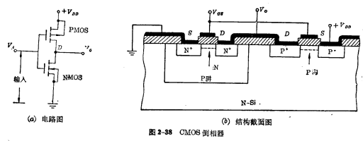
CMOS inverter is composed of an enhanced P-channel MOS tube and an enhanced N-channel MOS tube, where the NMOS tube is used as the input tube and the PMOS tube is used as the load Tube. The gates of the two tubes are connected together to lead to the input terminal; the drains of the two tubes are connected as an output terminal; the source of the load tube (PMOS) is connected to the power supply, and the source of the input tube (NMOS) is grounded. Working principle of CMOS inverter Figure 2-38 (a) is the circuit diagram of the inverter, and Figure 2-38 (b) is the cross-sectional view of the structure of the CMOS inverter. It uses diffusion method to form a low-concentration P-well region on a single N-type Si wafer, and then makes enhanced P-channel MOS tube and enhanced N-channel MOS on the N-type substrate and P-well region respectively. Tube, and finally use the method of steaming aluminum to form the electrode connection.

The working principle of CMOS inverter is like this, when input voltage , for the input Tube (NMOS),
  0, less than the threshold pressure
 , so the input tube is cut off, its cut-off equivalent resistance is very large; for the load tube ( PMOS),
 , the absolute value is greater than the threshold voltage< span style="font-size: 18px;">
 , so the load tube is turned on, and its equivalent resistance is very small. Since the pressure drop on the load tube is very small (approximately 0), the output voltage is
  . When input voltage
  (if equal to
  ), pair input tube,
  Greater than the threshold voltage
 , so the input tube is turned on, and its equivalent resistance is very small; the working principle of CMOS inverter for the load tube,
  , so the load tube is cut off, its cut-off equivalent resistance is very large, the power supply voltage
  Almost all land on the load tube, so the output is "0" level, which is approximately 0V.
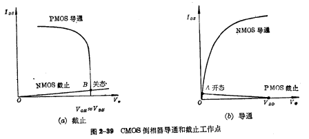
The characteristic curves of the two states of the inverter on and off are shown in Figure 2-39. Among them (a) is the cut-off characteristic curve of the CMOS inverter, and point B is the analog operating point; (b) is the turn-on characteristic curve of the CMOS inverter, and point A is the on-state operating point.

Contact: Mr. Zou
Tel: 0755-83888366-8022
Mobile: 18123972950
QQ: 2880195519
Address: 5C1, CD Block, Tianji Building, Tian’an Digital City, Chegongmiao, Futian District, Shenzhen
Please search WeChat Official Account: "KIA Semiconductor" or scan the following picture to "Follow" Official WeChat Official Account
Please "Follow" the official WeChat account: provide MOS tube technical assistance


