Electronic Technology Forum
Detailed analysis of the working principle and design considerations of MOS R-S tube trigger
Introduction to MOS triggers
Flip-flops and other logic components, In Chapter 2, we have introduced and gates, OR gates, and NOT gates. , "NAND", "NOR" and "AND or NOT" and other logic gates. The output of these logic gates is determined by the input state. If the input state changes, the output changes accordingly. Logic calculation and logic control can be realized by using these sequence-by-sequence gates. But these gate circuits do not have the function of "memory" signals. Once the input signal disappears, the output signal ceases to exist. In digital systems, circuits that count, shift, and store instructions and codes are also required, that is, these circuits are required to have the function of "memorizing" signals. The flip-flop is a circuit with a "memory" function. It has two stable states and can store the "1" and "0" of the binary code. Therefore, flip-flops can be used to form various complex logic circuits such as counters, shift registers, and memories. R-S tube flip-flops. This chapter mainly introduces the working principles and logical functions of various MOS flip-flops and other logic components, such as decoders, adders, shift registers, etc.
MOS R-S trigger
There are many types of triggers, such as RS triggers, JK triggers, D triggers, etc. according to function, and static triggers and standard triggers according to the working principle. Static trigger and dynamic trigger, but their logical structure is basically the same. The following will introduce the circuit structure of various flip-flops and their logical functions.
One, R-S trigger
1. Bistable trigger composed of two-stage inverter
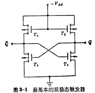
Figure 3-1 is a bistable state flip-flop circuit cross-coupled by two-stage PMOS inverters.In PMOS circuits, there are provisions for positive logic and negative logic. Here we use negative logic regulations to discuss the working principle of PMOS circuits.
In this PMOS circuit,
 Compose the first-stage inverter,
  < img src="/userfiles/images/2020/11/10/2020111014477790.png" title="image.png" alt="image.png"/> constitutes the second stage inverter. The output terminal of the first stage inverter is connected to the input terminal of the second stage inverter, the output terminal of the second stage inverter is connected to the input terminal of the first stage inverter, and the two output terminals are respectively Q and Q said.
This trigger has two stable states. A stable state is
 is on and
  until the end, another stable state is
  Turns on and
  is due. If there is no external influence, the circuit will stay in a certain stable state for a long time, so it is usually called a bistable flip-flop.
 In order to illustrate this feature of triggers, let’s first assume
 is turned on, and the output terminal Q is at the "0" level at this time. Since the output Q is connected to the input of another inverter,
  is off, make the output
  "1" Flat, the output terminal
  and
and  The gates are connected together again, which ensures that
  is on. If there is no external signal, this state will be maintained for a long time. This is the first stable state of the flip-flop.
 "Be good
 When it is turned on, the output Q is at "0" level, the same reason will make
  is cut off, the output Q is set to "1" level, this "1" level is added to
  On the grid, it is guaranteed that
  is turned on. This is another stable state of the flip-flop.
Usually put
 Is called "0" status, and
  is called "1 "state. It can be seen that the trigger can save the electrical signal "1" or "0" for a long time, and play the role of "memory" the electrical signal.
 If you want the trigger to change from one stable state to another stable state, you need to apply a signal to the trigger. Assuming that the trigger was originally in the "0" state, that is,
 , If the terminal is grounded, it will make
  cut off, making Q by "0" changes to "1", which causes
  to be turned on, Change Q from "1" to "0", and the flip-flop changes from "0" state to "1" state. This state transition is usually called the "flip" of the flip-flop.
 For the above flip-flops, Q and Q are both input and output, so they cannot be applied in actual circuits. The input terminal and output terminal of the flip-flop that can be applied must be separated. The following introduces various flip-flop circuits evolved from the simplest flip-flops described above.
2, basic RS trigger
RS flip-flop is also called set -reset flip-flop. The circuit is shown in Figure 3-2. This is based on the above double steady-state triggers, plus Two tubes, make
  separate
  are connected in parallel. In fact, it is composed of two inter-connected "or NOT" gate circuits. Q and
  also indicate two output terminals, R and S are two input terminals.
 (1) How it works
Assume that the trigger starts in the "0" state (

 ),Right now
 Conduction
 Deadline. In order to change the flip-flop from the "0" state to the "1" state, just keep the input terminal R at the "0" level, and add a "1" "level to the S end, because
 电平时,
电平时, Conduction,Make
 Output "0" level, and make
 Due,
Due, After cut-off, make Q become "1" level, and in turn make
 Conduction. In this way, even if the signal "1" on the S input is gone, the flip-flop will remain
 Arbitration,
 Conducted "1" state. Therefore, the input terminal S is called the set "1" input terminal, and it is also used as the set input terminal.
To restore the trigger from the "1" state to the "0" state, just keep the S terminal at the "0" level and add a to the B terminal The "1" level will do. Because when
 ,
,  is turned on immediately, changing Q from "1" to "0", and this "0" is entered into
  The gate of the tube
 The cut-off is due to the original
  is closed, so it changes from "0" to "1". The trigger is restored from the "1" state to the "0" state. Therefore, the R terminal is called the set "0" output terminal, also called the reset input terminal.
 In the RS trigger, if both the R and S input terminals maintain the "0" level, then
 are all closed, and the trigger remains in its original state. If both the R and S input terminals are added with "1" level, then
  are both turned on, the two output terminals Q and
  Have become "0" level, so that
  is closed, The normal state of the trigger is destroyed. When the two input terminals of R and S are restored from 1" level to "0" level, the state of the flip-flop cannot be determined. It is not certain whether it is in the "1" state or the "0" state. Therefore, in During the working process of the RS flip-flop, "1" level cannot be added to the two input terminals of B and S at the same time. The following is the logic diagram and truth table of the R-flip-flop.

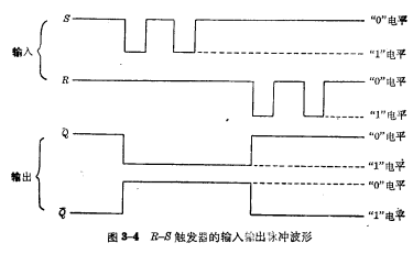
In order to better describe the working process of the R-S flip-flop, we have drawn its input and output pulse shape in Figure 3-4. It can be seen from the figure that adding a "1" level to the S terminal can make the flip-flop change from the "0" state to the "1" state, but if the flip-flop is already inIn the "1" state, adding a negative pulse to the terminal will not cause the flip-flop to change again. If you add at the R endThe "1" level can make the trigger change from the "1" state to the "0" state. If the trigger is already in the "0" state, adding a "1" level to the R input will not make the trigger anymore. Changes. It can be seen from Figure 3-4 that Q and
 The changes happen at the same time, which is an ideal situation. In fact, due to the delay effect,
 The changes in R and S are lagging behind.
(2) Design considerations
To make the circuit have the above two stable states, it must be correct Select the parameters and working conditions of each device in the circuit. Otherwise, the circuit cannot guarantee two stable working states and cannot realize the logic function of the flip-flop. The following describes the conditions and design ideas required for the normal operation of the circuit.①Maximum operating frequency
In order to make the RS trigger To work stably, the width of the trigger pulse must be greater than , so the trigger The highest frequency for is:
where
 It is the average transmission delay time of the first-level gate. The formula (3-1) gives the relationship between the highest operating frequency and the delay time of each logic gate that makes up the flip-flop. Therefore, during design, the delay time of each logic gate can be determined according to the requirements of the operating frequency, thereby determining the device parameters of each logic gate.
 ②Output level
To make the RS trigger keep working normally, the output Q (or
 ) must be less than the closing level of the gate circuit, and the absolute value of the "1" level must be greater than the opening level of the gate circuit , So that the gate circuit is reliably cut off and fully turned on, so as to ensure that the trigger is in a stable working state. According to this requirement, the transconductance ratio of the gate circuit load tube and input tube can be determined.
 ③Static power consumption
RS trigger is dual The steady-state circuit is composed of the two gates of the flip-flop. One gate is always turned on and the other gate is turned off during operation. Therefore, only one gate can be considered when calculating the static power consumption of the flip-flop. Like the design of an inverter, power consumption and speed are contradictory, and they are related to the geometric size of the load tube.(3) Features of basic RS triggers
From the above analysis, it is known that it is formed by connecting two NOR gates. The circuit is symmetrical and the structure is simple. It is the basis of other flip-flops. Its characteristics are:①It has two stable working conditions and the function of "memorizing" information.
②The function of setting "0" or "1" can be achieved by adding negative pulses to the R and S input terminals respectively. However, the storage of the R-S flip-flop state cannot be controlled in time, and it is difficult to directly apply it in medium and large-scale integrated circuits where various units must cooperate with each other. Moreover, the R-S flip-flop only has the function of setting "1" to "0", and the R and S terminals cannot be "1" pulses at the same time. Therefore, the basic R-S flip-flop must be continuously improved to make it have perfect functions.
3, RST burner
When using a trigger in a computer, a pulse is often used to control the flipping time of the flip-flop. This kind of pulse that controls the flipping time of the flip-flop is called a clock pulse, and the commonly used symbol is
 to indicate. Only when the clock pulse is input, the flip-flop will determine its state according to the level on the input terminal; when there is no clock pulse input, no matter how the state on the input terminal changes, the flip-flop will not change its original state.
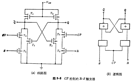
 The RS-T trigger (or synchronous trigger) shown in Figure 3-5 is the
 controlled by RS to trigger the device, which is the same as RS Compared with the flip-flop circuit, there are two more
  two MOS tubes, Their gates are all controlled by clock pulses. If
  is
is  can not be turned on, R and S can not work, the trigger will not change the original state. Only when
  is "1" level,
  is turned on, at this time RS is the same as the aforementioned trigger, completing the trigger Logic function.
4. Master-slave RS trigger
Although the structure of the RS trigger mentioned above is simple, But its performance is not perfect, it can't count, it can't constitute a shift register. In order to improve the performance of the trigger, further improvements are needed. For this reason, an RS flip-flop with a master-slave structure has been developed, which can make external information in the clock pulse. is sent to the main trigger for temporary storage within the time of action, and then in the opposite clock pulse (called complementary clock pulse
  ), transfer the information stored in the master trigger to the slave trigger.
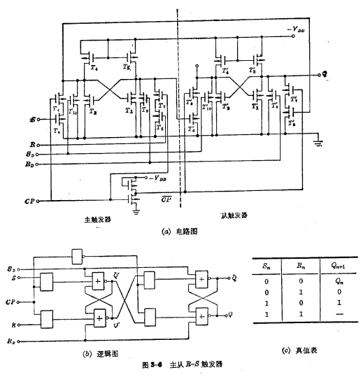
 Figure 3-6 is a master-slave trigger composed of two independent R-S-T triggers. The left one is the master trigger and the right one is the slave trigger. The connection method is to connect the Q' of the main trigger and
 The terminals are respectively connected with the S' and R' terminals of the slave trigger. Where
  and
and  Preset position tube for master and slave triggers,
  is the preset input terminal. When
 , the master-slave trigger is in the "0" state.
  and
and  is respectively subject to
  and
and  pulse Controlled device. Because of
  and
and  The control isolates the master and slave flip-flops, eliminating the trigger period during a clock pulse. Somersaults with multiple flips may occur.
 Let’s analyze the function of the master-slave R-S trigger. When the clock pulse CP changes from "0" to "1", the state change of the main flip-flop is the same as the single R-S flip-flop mentioned above. At this time, because
 changed from "1" to "0", < img src="/userfiles/images/2020/11/10/2020111016305642.png" title="image.png" alt="image.png"/> is changed from on to end, so the state of the trigger remains unchanged. When
  changes from "1" to "0",
  The tube ends, at this time the main trigger will store the original signal, At the same time, because
  changed from "0" to "1",
  is turned on, and the state of the master trigger can be transferred to the slave trigger.
When designing a circuit, the W/L of each device of the master flip-flop is generally smaller than that of the corresponding slave flip-flop, because As long as the master trigger drives the slave trigger, the load is not large. However, the output from the flip-flop generally needs to be connected to a larger load, so the W/L of each device from the flip-flop will increase. When the load connected to the output terminal is very large, it is necessary to add another driver at the output terminal, otherwise the area occupied by the chip from the flip-flop will be too large.Contact: Mr. Zou
Tel: 0755-83888366-8022
Mobile: 18123972950
QQ: 2880195519
Contact address: 5C1, CD Block, Tianji Building, Tian’an Digital City, Chegongmiao, Futian District, Shenzhen
Please search the WeChat official account: "KIA Semiconductor" or scan the picture below to "Follow" the official WeChat official account
Please "follow" the official WeChat public account: provide MOS tube technical assistance


