Electronic Technology Forum
DC transmission characteristics and noise tolerance of CMOS inverters
CMOS inverter transmission characteristics
First, DC transmission characteristics and noise tolerance
CMOS transmission characteristics
As you all know, the transmission characteristic curve of an inverter can be derived from the current equations of the two tubes of the inverter to derive the corresponding relationship between the input voltage and the output voltage, and then make Pictured.
For the convenience of discussion, let’s first explain the conditions under which the load tube and the input tube work in the saturation zone or exhaust saturation zone. Figure 2-40 shows the voltage offset between the negative limit tube and the input tube. Transmission characteristics of CMOS inverter
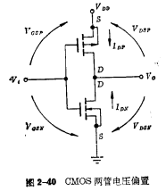
It can be seen from the figure that for the input tube (NMOS), its working state is in the boundary between the saturated and unsaturated regions:

where
When When, NMOS works in the unsaturated zone;
 , the work is saturated Area.
For the load tube PMOS, its working state is in the saturated zone and non-saturatedThe dividing line between the zone is :

where
When When, PMOS works in the unsaturated zone,
 , the work is in the saturation zone.
Therefore, the current formula of the two devices in two states can be written:


Visible when  When rising from 0V to
  , the load tube and input tube will be In different working conditions, because of the output voltage of the inverter
  also Change accordingly. For the sake of intuition, let’s first give an input voltage
  rising from 0V to A practical example of 10V to illustrate the relationship between the output voltage and the input voltage. The transmission characteristics of the CMOS inverter assumes that the two tubes are completely symmetrical, with
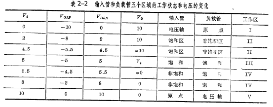
  , when the input voltage rises from 0V to 10V, the working status of the input tube and the load tube and the change of the output voltage can be divided into five areas for discussion.
District I city:  , the input tube ends; and
  , the load tube guide Pass.
At this time Ip=0, output voltage , as shown in Figure 2-41(a).
Region II:  , the input tube is turned on and working in the saturation zone; at the same time,
 , the load tube is also turned on, working in the unsaturated zone . At this time,
  , the output voltage meets:
  , as shown in Figure 2-41(b).
Region III: When  , there are still
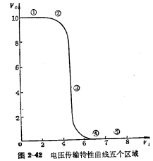
  , input tube and load tube are both Turn on, and all work in the saturation region. At this time, Ip is the largest and Vo drops sharply. This area is called the high gain area (also known as the conversion area). At this time, the corresponding input voltage is called the conversion level, which is used
  means, as shown in Figure 2-41(c).
Region IV:  ,
,  , the input tube is turned on, working in non Saturation zone, at the same time,
  , the load tube is also turned on, working in Saturation zone,
  is better than
  , the output voltage meets
  . As shown in Figure 2-41(d).
Region V:  , the input tube is on, but
  , the load tube is off ; At this time
  , as shown in Figure 2-41(e) .

According to the various working points of the above output characteristics, the corresponding  The relationship curve, as shown in Figure 2-42, is the transmission characteristic of the CMOS inverter.
Although the above analysis results are obtained from the simplified strips of symmetry complementary pipes, they can Have a comprehensive understanding of the entire working process of the inverter. The transmission characteristics of CMOS inverters are for asymmetric devices (ie 
 ) The transmission characteristics of the inverter composed of the current equation Start, get a general expression.
As seen in Figure 2-40, the current through the load tube and the input tube are equal, namely:

In Area I: Because the input tube is cut off, because 
ie:
So:
In II Zone: PMOS works in the unsaturated zone, and NMOS works in the saturated zone. Because

so:
After sorting out, you can get:

in IIIZone: Both PMOS and NMOS work in the saturation zone.
so:
After sorting, it can be solved:

If the two tubes are perfectly symmetrical under ideal conditions, there will be
In the TV zone: PMOS works in the saturated zone, and NMOS works in the unsaturated zone, so according to 

In Zone V: Because the load tube is cut off, due to 

so:
Through the above analysis, it can be seen that the CMOS inverter has the following characteristics:
❶Logical swing is large and high level Up to
Up to  , low level< img src="/userfiles/images/2020/11/04/2020110416023174.png" title="image.png" alt="image.png"/> can be approximated to 0. In this way, the power supply voltage is fully utilized, and a lower power supply voltage can be used.
❷The voltage gain of the conversion area is high when the conversion level is  , the output voltage drops quickly, so it can tolerate a larger noise voltage than, and the anti-interference performance is better .
❸Low power consumption Whether it is outputting high level or low level, one of the two tubes is always in the cut-off state, there is no direct path between the power supply and the ground, but only PN The leakage current of the junction passes. The transmission characteristic of the CMOS inverter therefore the operating current Io is very small, approximately zero. Therefore, CMOS static power consumption is extremely low, generally on the order of nW. Because of this, CMOS circuits are also called micro-power circuits.
CMOS noise tolerance
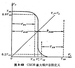
In CMOS circuits, for design convenience, the definition of maximum noise tolerance is generally used. It corresponds to the intersection of the DC transmission characteristic curve and the line  The difference between the input voltage and the power supply
  and zero potential, respectively, to represent Noise tolerance for high and low levels. Since the MOS inverter has a very high voltage gain in the conversion area, the input voltage corresponding to the intersection point is the conversion level.
 , as shown in Figure 2-43shown.
Low level maximum noise tolerance:

High level DC noise tolerance:

As seen from Figure 2-43, the maximum noise tolerance is obviously higher thanGo to the defined designation Noise tolerance  and
and  must be large, only When the transmission characteristic becomes the ideal characteristic curve, the two are approximately equal.
According to the definition of the maximum noise margin, we know that to get a larger noise margin depends on the conversion level The size. So it is necessary to discuss the influence of various factors in the conversion level on the transmission characteristics.
All the parameters in the formula (2-68) are correct. Perform normalization and introduce normalization parameters. Order:
 < span style="font-size: 18px;">For the normalized conversion level
 , Is the threshold voltage of the normalized PMOS tube
 < span style="font-size: 18px;">, is the threshold voltage of the normalized NMOS tube
 K factor of PMOS tube to NMOS tube Than
So (2-68) is written as normalization Form
If the two tubes are symmetrical, it means  , the ideal maximum noise voltage can be obtained as 1
 .
.
Actually,  not equal to
  ,
, is not equal to
  , so
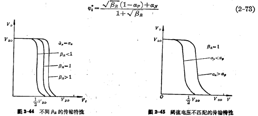
, so  to reduce the noise margin. Figure 2-44 shows the influence of different
  on the transmission characteristics, the figure 2-45 represents the influence of the different threshold voltages of the two tubes on the transmission characteristics. In the design of the transmission characteristics of the CMOS inverter, in the case of
  , In order to make
  as close to 1/2 as possible, adjustment is often used< img src="/userfiles/images/2020/11/04/2020110416155054.png" title="The transmission characteristics of the CMOS inverter" alt="The transmission characteristics of the CMOS inverter"/> size (that is, adjust the two tubes The geometric size ratio) to achieve.
Contact: Mr. Zou
Tel: 0755-83888366-8022
Mobile: 18123972950
QQ: 2880195519
Address: 5C1, CD Block, Tianji Building, Tian’an Digital City, Chegongmiao, Futian District, Shenzhen
Please search WeChat Official Account: "KIA Semiconductor" or scan the following picture to "Follow" Official WeChat Official Account
Please "Follow" the official WeChat account: provide MOS tube technical assistance


