Electronic Technology Forum
CMOS gate circuit (NAND gate, NOR gate, NOT gate, transmission gate, etc.) detailed introduction
1. CMOS NAND gate and NOR gate circuit
Figure 2-68 shows the CMOS NAND gate circuit, where  is two NMOS tubes connected in series,
  are two PMOS tubes connected in parallel,
  and
and  The poles are connected together as the input terminal
 ,
, and
and  The gate connection is used as the input terminal
 , the omission of
 The missing link leads to the output terminal F. When both A and B are input as "1" (VDD),
  Turn on,
  Turns off, and the output is "0" level; When either input between A and B is "0" level, two N tubes in series
 There is no path to the ground, and two P-tubes connected in parallel always have one conduction, the equivalent on-resistance is very small, and the power supply voltage almost all falls on
  On the tube, so the output is "1" level; when A and B are all "0" level , Until
  is turned on, the output is still high level "1" . So the circuit has the logic function of "NAND".
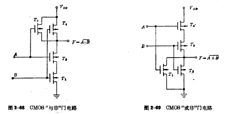
Figure 2-69 shows the "NOR" gate. Its connection method is just the opposite of the "NAND" gate. Two N tubes is in parallel, two P tubes
 is concatenated. As long as there is an input "1" level at input A or B, the NMOS will have a conduction, and the output will be at "0" level. Only when A and B are both "0", make
  will be cut off before outputting the "1" level. So the circuit has the logic function of "NOR".
If an inverter is added behind the NAND gate and the NOR gate, it will form a CMOS AND gate and a CMOS OR gate circuit.
2, CMOS "and-or-not" gate
Figure 2-70 shows the CMOS NAND gate circuit, which is composed of three NMOS tubes as the input tube, and three PMOS tubes as the load tube. The connection method of the input tube is the same as that of the single-channel AND NOR gate. The connection method of the three load tubes is  in parallel, and then connected with
  in series. The connection method of the grid is the input tube in series
 Load tubes connected in parallel with each other
 Connect together to form A and B input terminals, parallel input tubes
 Connect with the serial load tube
  to form
  input terminal.
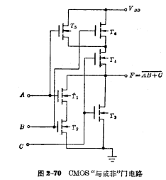
It can be seen from the above discussion that when the CMOS gate circuit has multiple input terminals, each input tube branch is in series, and its corresponding load tube branch is parallel.Joint form. On the contrary, if each input tube branch is in parallel, the load tube isTandem form.
3. Consideration of the geometric size of CMOS interconnect and parallel gate devices
inIn the discussion of the noise tolerance of CMOS inverters, it is known that to obtain the maximumDC noise capacity must meet conditions of. For multi-input"NOR" and "NAND" gates (or parallel or series gates), which
 Factors need to be used separately
 Effective and
 There are numbers to express; to get the maximum noise capacity, you must meet
 natural conditions.
The principle of determining the size of NOR gates and NAND gates is discussed below:
(1) The device size of the NOR circuit when the input tube is a parallel gate, as shown in Figure 2-69. If the two N tubes are fully turned on, the on-resistance of the two tubes in parallel is 1/2 of that of a single tube, ie  , because of

So, you can get  . But usually as long as any one of the two parallel tubes is turned on, the gate circuit can output "0"
Level. So there are

When the input tubes are connected in parallel, the load tubes are connected in series. If two P tubes connected in series are turned on at the same time, their on-resistance is twice that of a single tube, that is  , so you can get

According to the conditions required to obtain the maximum noise capacity,

If there are  input terminals, there are:
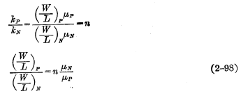
If you take  , then:

The (2-100) formula shows that in  input In the NOR gate circuit at the end, the channel width of the series device (load tube) is similar to that of the parallel device (input tube)
  times (think
  ).
).
(2) The device size of the "NAND" gate circuit is similar to the above method, which can be based on  conditions, get;

The (2-101) formula shows that in  input In the NAND circuit at the end, the channel width of the series device (input tube) is about% times that of the parallel device (load tube) (think
4, CMOS buffered output
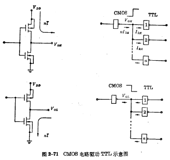
Most CMOS devices have relatively high output impedance, which limits the ability to supply or sink current, so they are completely suitable for driving CMOS circuits. However, when you need to drive a TTL circuit, you need to provide a larger drive current or sink current (Figure 2-71). Therefore, a dedicated circuit with a low impedance output must be designed. The form of this circuit is the same as a typical CMOS inverter, but the size of the device is much larger than a standard CMOS transistor. The size of the device can be determined from the current equation according to the drive current or sink current.
5. CMOS three-state output circuit
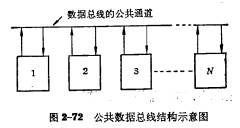
In the transmission of many data, it is often necessary to supply signals from various points to a common output line, As shown in Figure 2-72. So can the output terminals of each CMOS circuit be directly connected together as shown in Figure 2-73? Obviously it is not possible.
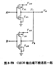
As can be seen from Figure 2-73, if the output of inverter A  is "1" level, the output terminal of inverter B
 is "0" level, then
  And
And  is turned on, from the power supply VDD has a path to the ground. Because of
  and
and  The lead resistance is relatively high, and the two are almost equal, so V is output. Will be
 , neither high nor low. Therefore, the output state cannot be determined.
In order to realize the connection as shown in Figure 2-72 on the common bus, the CMOS circuit needs to have the function of three-state output. The so-called three-state output means that the output state of the circuit not only has high-level and low-level output, but also has a third state (or high-impedance state). When the circuit is in the third state, the load tube and the input tube are both in the cut-off state, and its logic level is determined by the output state of other logic gates connected in parallel with it on the common bus. When the circuit is in the third state, its output terminal is isolated by the high-impedance devices that are all cut off, so it has no definite state, nor will it affect other circuits.
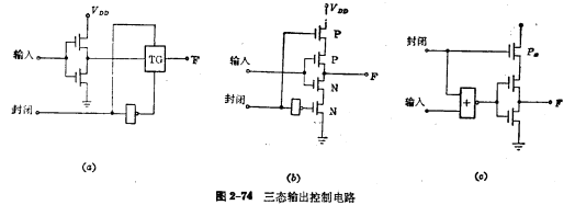
The CMOS circuit can easily realize the tri-state output function. Figure 2-74 shows several ways to realize the tri-state output.
In Figure 2-74(a), a transmission gate is connected in series with the output terminal. When the transmission gate is turned off, F and the output circuit are disconnected. When the transmission gate is turned on, the state of point F changes with the input of the inverter.
In Figure 2-74(b), when the inhibit signal is high, the additional P and N tubes connected in series with the inverter are both cut off, effectively cutting off the power supply VDD, make the inverter in the third state; when the closed signal is low, the two additional P and N tubes are both turned on,F The state of the dot changes with the inverter.
In Figure 2-74(c), when the closed signal is high,  is off, no matter what signal the input terminal is, the output of the "NOR" gate of the inverter gate is low,
  At the end, the inverter is in the third state. When the closed signal is low,
  is on, F changes with the inverter.
The three-state output circuit is not only used in simple gate circuits, but also often used in more complex circuits.
When the output of a tri-state device is closed, it has a parasitic capacitance similar to a typical CMOS input capacitance. Its value is about 10~15pF. Therefore, in the drive of any device in Figure 2-72, the bus must charge all the input and output capacitors connected to it and the capacitors of all the connecting lines, so that the circuit reduces the operating speed, except for the delay caused by the capacitance. , Must also consider the turn-on and turn-off time required by the prohibition circuit.
Contact: Mr. Zou
Contact number: 0755-83888366-8022
Mobile phone: 18123972950
QQ: 2880195519
Address: 5C1, CD Block, Tianji Building, Tianan Digital City, Chegongmiao, Futian District, Shenzhen
Please search WeChat Official Account: "KIA Semiconductor" or scan the following picture to "Follow" Official WeChat Official Account
Please "follow" the official WeChat account: provide MOS tube technical assistance


