Electronic Technology Forum
CMOS inverter transient response analysis and detailed explanation
CMOS invertertransient response
From the analysis of the transient characteristics of the single-channel MOS inverter, it is known that the frequency response of the MOS tube that composes the inverter is relatively fast. In the actual circuit, the main factor that affects the switching speed of the circuit is the load capacitance at the input  and the size of the MOS device's ability to charge and discharge these capacitors.
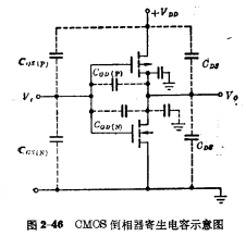
Figure 2-48 is a schematic diagram of various parasitic capacitances in a CMOS inverter. Here a total effective load capacitance is used. to indicate.

In the formula Is the input capacitance, including gate-source capacitance and gate
 drain capacitance;
  indicates output capacitance, including drain-substrate junction capacitance and package wiring Wait for stray capacitance. The coefficient
  means the driver
  The same inverter.
When discussing the switching characteristics of CMOS inverters, it is still assumed that the inputthe input voltage is the ideal level Leap wave.
1. Fall time (on time)
CMOS inverterThe fall time analysis method is the same as that of E/EMOS of. When the input changes from "0" to "1" (set input "1" level equal to  ), the inverter should achieve "0" level output,
  must be discharged through the saturated and non-saturated regions of the input tube, as shown in Figure 2-47 (a). The discharge trace is shown in Figure 2-47 (b).
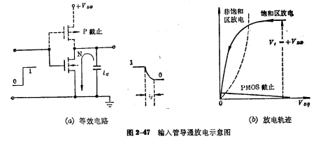
(1) Discharge time in saturation zone
When , The input tube works in the saturation zone. Since the load tube is cut off, the load tube current can be ignored
  . According to
  (saturated), the equation is obtained:

Use the method of separating variables to integrate. During this discharge time, the voltage drops from  to
to  (saturation and non-saturationthe dividing point of the saturation zone).

This is the load capacitance when the CMOS inverter is turned on. The time required to discharge the input tube working in the saturation zone.
where:

is called the time constant.
If , Can be counted as:

(2) Discharge time in unsaturated zone
When When the input tube works in the unsaturated zone, the discharge trajectory corresponds to a section of the curve in the unsaturated zone. Similarly, according to
  , the equation can be obtained:

Use the method of separating variables to integrate. During this discharge time, the output voltage drops from  to
to  , that is, output "0" level.

Use the integral formula:

get:

This is the inverter load capacitance The time required to discharge the input tube working in the non-saturated region.
When , Can be calculated as
  .
.
(3) Fall time expression
The fall time of the CMOS inverter should be the sum of the discharge time in the saturated zone and the discharge time in the unsaturated zone:

If written in the form of normalized voltage, the fall time can be expressed as:
 < /span>
From the formula (2-82), we can see that the fall time of the CMOS inverter is proportional to the load capacitance,
  The larger the discharge time, the longer the discharge time, and the channel width to length ratio of the input tube (W/L)N, Inversely proportional, (W/L) Nheal is small, the input tube etc. The greater the effective resistance, the longer the discharge time.
2, ascent time (cut-off time)
When the input of the CMOS inverter jumps from "1" to "0", the circuit changes from on to completely off. In order to reach the "1" level  output, the load tube turned on The capacitor
  must be charged, as shown in Figure 2-48.
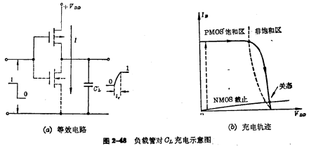
The same as the method of analyzing the fall time, the expressions for the time constant and fall time are:

Written as normalized rise time:

From the formula (2-86) we can see that the rise time of the CMOS inverter and load capacitance
 is proportional to the channel width to length ratio of the load tube
 Inversely proportional.
Because when the CMOS inverter is on or off, one tube is always cut off and the other is on. Therefore, the channel size of the load tube is not limited by power consumption. Therefore, the width-to-length ratio of the load tube and the input tube channel can be designed to be similar.
In this way, the capacitor can be made  The charging and discharging times are almost the same, and the rise time and fall time are also approximately equal. This is different from the case of a single-channel MOS inverter.
Equations (2-82) and (2-86) are derived when the input is a step wave. The relationship between the normalized rise or fall time and the normalized threshold voltage can be shown in Figure 2-49. Since the two expressions are completely symmetrical, the horizontal axis represents  When, the vertical axis represents the normalized fall time, such as the horizontal axis represents
  , the vertical axis represents the normalized rise time.
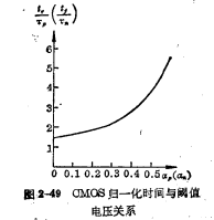
It can be seen from the figure that the higher the threshold voltage, the slower the switching time.  When the voltage relationship exceeds 0.3, the switching time increases significantly with the increase of the threshold voltage.
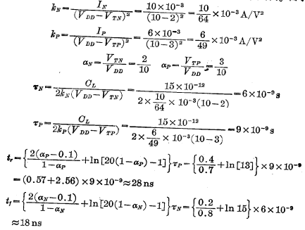
In order to have a quantitative concept of the switching time of CMOS inverters, here is an example.
Assuming the total load capacitance of the CMOS inverter Saturation current measured separately
 ,Find the switching time of the inverter. Because:
3、双门延迟时间
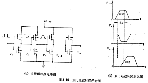
Because the output signal of the inverter not only has a certain rise and fall time, but also has a certain time delay relative to the input signal, which is called delay time. Figure 2-50 (a) shows a multi-stage inverter. Even if a step voltage signal is input to the first stage, its waveform will not be guaranteed to be a step signal after several stages. When such a non-step signal drives the next-stage inverter, obviously the delay time will be longer.
The so-called double-gate delay time refers to the time interval of the corresponding 50% amplitude after the input voltage passes through the two-stage inverter, also Called "right" delay time, its approximate expression is:
>

This style is in  , which is only applicable in the case of approximate matching. Use this formula to calculate
  , the error is not more than 10%.
It can be seen from Figure 2-30: " is short, the rise and fall times of the inverter must be short. The rise time is mainly related to the load tube, and the fall time is mainly related to the input tube. If the rise time is very short, the fall time Very long, obviously can not shorten the delay time of the double gate, on the contrary, if the fall time is very short, and the rise time is very long, it cannot be used." shorten. To make
  The shortest condition must be met
 , and both are very small . In order to meet this requirement, the parameters of the inverter must meet the approximate formula:

If the two tubes are completely symmetrical, obviously is the best switch response condition. If
  , the switching performance of the circuit will deteriorate. With the decrease of
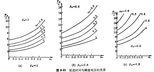
  , the switch response worsens. Refer to Figure 2-51 for details. The figure shows when
  ,
,  and
and  relationship. When
  decreases, due to the decrease of the transconductance of the load tube, the PMOS The charging time of the load tube for
  becomes longer, making
  At the same time, as the valve voltage increases
 increases, so it leads to
  increased. Therefore, in the speed design, it is emphasized that
  , and the threshold voltage should be small Is very important. For example, if
  is very small, the load control
  will affect
 , the load tube is difficult to conduct, resulting in
  increases, so the switching characteristics become worse and the delay time becomes longer.
Contact: Mr. Zou
Tel: 0755-83888366-8022
Mobile: 18123972950
QQ: 2880195519
Address: 5C1, CD Block, Tianji Building, Tian’an Digital City, Chegongmiao, Futian District, Shenzhen
Please search WeChat Official Account: "KIA Semiconductor" or scan the following picture to "Follow" Official WeChat Official Account
Please "Follow" the official WeChat account: provide MOS tube technical assistance


