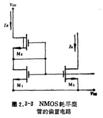
The bias circuit analysis and interpretation process of NMOS transistors. There are two types of bias circuits for NMOS transistors. One is the bias circuit with an enhanced transistor as the equivale
The bias circuit analysis and interpretation process of NMOS transistors. There are two types of bias circuits for NMOS transistors. One is the bias circuit with an enhanced transistor as the equivale
MOS tube bias circuit.In MOS analog integrated circuits, the bias circuit is an indispensable and important part. The bias circuit is closely related to the constant current source circuit in the pre
MOS tube bias circuit.In MOS analog integrated circuits, the bias circuit is an indispensable and important part. The bias circuit is closely related to the constant current source circuit in the pre
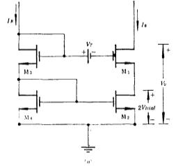
Constant current source circuit. Although the above-mentioned improved constant current source circuit increases the output impedance and improves the constant current performance, when used as an act
Constant current source circuit. Although the above-mentioned improved constant current source circuit increases the output impedance and improves the constant current performance, when used as an act

The characteristics of Wilson constant current source are shown in Figure 2.2-4. Due to the effect of negative feedback, the circuit has high output impedance and good constant current characteristics
The characteristics of Wilson constant current source are shown in Figure 2.2-4. Due to the effect of negative feedback, the circuit has high output impedance and good constant current characteristics

The constant current source circuit with high output impedance is shown in Figure 2.2-2. Compared with the constant current source circuit in Figure 2.2-1, MOS transistors M2 and M4 are added. Due to
The constant current source circuit with high output impedance is shown in Figure 2.2-2. Compared with the constant current source circuit in Figure 2.2-1, MOS transistors M2 and M4 are added. Due to
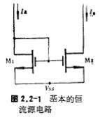
MOS constant current source circuit In MOS analog integrated circuits, the constant current source circuit is often used as a bias circuit and as an active load of an amplifier. The performance of ana
MOS constant current source circuit In MOS analog integrated circuits, the constant current source circuit is often used as a bias circuit and as an active load of an amplifier. The performance of ana
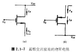
Active resistance analysis of MOS field effect transistor connection mode 1. Source AC grounding Figure 2.1-6a and b respectively represent the active resistance of the source AC grounding of the N-ch
Active resistance analysis of MOS field effect transistor connection mode 1. Source AC grounding Figure 2.1-6a and b respectively represent the active resistance of the source AC grounding of the N-ch

N-channel depletion type is used as an active resistor, and its connection mode (ie, gate-source short-circuit) and V-I characteristics are shown in Figure 2.1-4 and b respectively. N-channel depletio
N-channel depletion type is used as an active resistor, and its connection mode (ie, gate-source short-circuit) and V-I characteristics are shown in Figure 2.1-4 and b respectively. N-channel depletio

MOS transistor gate-drain active resistance, the main application of MOS field effect transistors in MOS analog integrated circuits has the following three aspects: one is as an active load of the amp
MOS transistor gate-drain active resistance, the main application of MOS field effect transistors in MOS analog integrated circuits has the following three aspects: one is as an active load of the amp
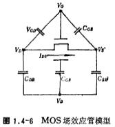
Short-channel MOS threshold voltage model, the main parameter relations and process parameters of MOS field effect transistors are as follows (see reference [12]), which is the diffusion depth (juncti
Short-channel MOS threshold voltage model, the main parameter relations and process parameters of MOS field effect transistors are as follows (see reference [12]), which is the diffusion depth (juncti


5C1, CD Block, Tianji Building, Tianan Digital City, Futian District, Shenzhen

KIA-The Public