Electronic Technology Forum
The influence of MOS tube substrate bias effect (body effect) on threshold voltage
MOS tube substrate bias effect
In a MOS integrated circuit composed of many MOS tubes, many tubes are built on the same substrate. At this time, it is impossible to connect the sources of all MOS tubes to a common substrate, and the substrate of some tubes is bound to increase relative to the source. A reverse bias voltage ,due to
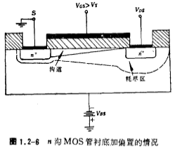
 the influence of voltage increases the turn-on voltage of the enhancement mode MOS tube, and causes the depletion mode tube to change in the direction of the enhancement mode tube. The biasing of the n-channel MOS tube substrate is shown in Figure 1.2-6.

After the reverse bias voltage is applied between the substrate and the source of the MOS, the width of the depletion region between the channel and the substrate becomes larger, and the number of negatively charged ions increases, so that there are more negative charges in the depletion region. MOS tube substrate bias effect. At the same time, since the gate voltage has not changed, the positive charge domain on the gate has not changed. According to the principle of charge conservation of the entire system, the total amount of negative charge on the silicon surface should not be changed. It can be seen that the increase of the negative space charge in the depletion zone will inevitably reduce the electron charge density in the channel, thus leading to the weakening of the channel's conductivity. To maintain the original electron charge density in the channel to maintain its conductivity, it is necessary to increase the gate voltage VGS to increase the total amount of positive charge to compensate for the increase in negative charge in the space charge region caused by image.png. The turn-on voltage of the n-channel MOS tube is increased accordingly. MOS tube substrate bias effect. Obviously, the greater the VBS, the greater the increase in turn-on voltage ΔVT. Let's discuss ΔVT below.
Due to reverse bias the depletion layer between the channel and the substrate expands to the inside of the substrate, and the charge in the depletion layer increases, which is similar to the formula (1.2-6), which can be expressed as:

Its threshold voltage is:

(1.2-16) minus (1.2-12) formula, we get ΔVT:

where

Called body effect factor. thereby:

For P-channel enhanced MOS tube, ΔVT<0, that is:

Contact: Mr. Zou
Contact number: 0755-83888366-8022
Mobile phone: 18123972950
QQ: 2880195519
Contact Address: Block 5C, CD Block, Tianji Building, Tianan Digital City, Chegongmiao, Futian District, Shenzhen
Please search WeChat official account: "KIA Semiconductor" or scan the following picture to "Follow" official WeChat official account
Please "follow" the official WeChat account: provide MOS tube technical assistance


