Electronic Technology Forum
Analysis and explanation of the DC characteristic model of MOS FET
DC characteristics of MOS FET
Removal of the image The five capacitors in 1.3-1b are the DC characteristic models of n-channel MOS transistors. The model except ohmic resistance outside, only for drain-source current IDand two substrate junction diodes for simulation.
From the discussion in the first section, we can see that the MOS field effect transistor can be divided into linear region (adjustable resistance region) and saturation region.
Take the n-channel enhancement mode MOS as an example to discuss the current-voltage characteristics of the MOS tube before the channel is pinched off (that is, in the linear region). In the linear region, the drain voltage VD is smaller than the gate voltage VG. The three-dimensional view of the n-channel MOS tube is shown in Figure 1.3-2. An inversion layer channel is formed from the source to the drain. The width W of the channel and the length L of the channel are fixed values. The thickness of the channel is  is smaller than the oxide layer thickness tox, the three-dimensional picture of the channel is on the right side of the figure, and the Y direction is the current ID's flow direction.

Suppose the current density of the channel is J(x,y), then the drain-source currentI< span style="font-size: 10px;">D is:

Because of 
and V is the channel voltage, which is a function of х and у.
Substituting (1.3-2) formula into (1.3-1) formula is obtained

The above formula n is the electron concentration in the channel, μn is the electron mobility.
Because of Very small, in the direction of
  the channel voltage V can be approximated as Therefore, the channel voltage V is only a function of y, and assuming that the electron mobility in the channel is also constant, the above formula can be written as:

and  Channel electron charge per square centimeter = gate charge-VT induced charge:

Substituting the above formula into (1.3-4) formula:

Integrate both sides of the above formula to get:

From the above formula

In the formula, μn is the average mobility of electrons in the channel, and the unit is cm 2 (V·sec);
 = Gate oxide capacitance per unit area, the unit is method/cm2;
 Is the vacuum permittivity, and its value is 8.85×10⁻¹⁴ method/cm;
 is the relative permittivity of the gate dielectric SiO2, its value is 3.8~4;
 is the thickness of the gate oxide layer, and its value is generally 600~1000 angstroms; W is the channel width; L is the channel length; the threshold voltage VT is expressed as:
Where VT refers to therefore, VT is called the zero-bias threshold voltage, and its value is determined by the following formula:

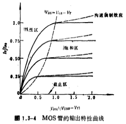
If it is assumed that the threshold voltage VT is a certain value (such as VT=1), the ID~VDS relationship curve can be drawn without using the formula (1.3-6). The curve is shown in Figure 1.3-3, corresponding to a certain VGS, ID has A maximum value, VDS=VGS-VT at the maximum value. That is, when VDS≥VGS-VT, it is no longer in the linear zone, but enters the saturation zone. When VDS increases to When the drain-source voltage is reached, the channel at the drain end starts to be pinched off, that is, the induced channel at the drain end disappears. The direct current characteristic of MOS field effect tube. In this way, the formula (1.3-6) is no longer applicable. After entering the saturation zone, ID basically remains unchanged, it can be determined by the VDS in the formula (1.3-6)
 substitute in and get


After entering the saturation region, due to the existence of a barrier region between the drain region and the pinch-off point of the channel (see Figure 1.1-9c), the effective length of the channel is shorter than that when it is not pinched off. This effect is called the channel Length modulation effect. Set the channel length shortening value to ΔL, then the effective channel length affected by the modulation is:

The ΔL in the formula can be expressed by the following formula:

It can be seen from the formula (1.3-11) that the shortening of the channel length ΔL is related to the drain-source voltage VDS. The greater the VDS, the greater the width of the barrier between the drain region and the channel pinch point, that is, the greater the ΔL. Effective channel length the smaller.
The channel length modulation effect causes the saturation region current to increase with the increase of the drain-source voltage VDS, which reduces the drain-source output impedance of the MOSFET.
To reflect the channel length modulation effect after the MOSFET enters the saturation region. As long as the L in the formula (1.3-9) is used in the formula (1.3-10) just replace it. Its relational expression is written as:

where , Is the channel length modulation parameter, the unit is volt-1. (1.3-13)

Using (1.3-6) and (1.3-12), the output characteristic curve of the MOSFET is shown in Figure 1.3-4. For clarity, normalized coordinates are used in the figure. when
 . In the saturation zone,
 Represented by a solid line;
 It is represented by a dashed line.
In summary, the working area of MOSFET can be divided into three areas, namely cut-off area, linear area and saturation area. The current-voltage relationship of each area is:
1、Cutoff area

2、Linear region


3、Saturation zone

The VT in (1.3-14~16) is still expressed by the formula (1.3-7).
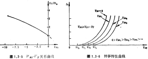
From the formula (1.3-7), the threshold voltage VT and the reverse bias voltage between the substrate and the source related, when VDS=0,
 ,With reverse bias
 increase, VT also increases. This VT varies with
 the effect of increasing and increasing is usually called the substrate bias effect or the body effect.
 the relationship curve can be shown in Figure 1.3-5, and its transfer characteristic curve (ID-VGS) is shown in Figure 1.3-6.
In circuit and layout design, the source of the MOS tube is usually connected to the substrate to avoid substrate bias effects.

Because the MOS field effect tube is symmetrical, the n-channel MOSFET can work in the forward region, that is, VDS>0, or in the reverse region, that is, VDS<0. When working in the reverse zone, its effect is equivalent to that the drain of the forward zone becomes the source of the reverse zone, and the source of the forward zone becomes the drain of the reverse zone. The direct current characteristic of MOS field effect tube. The current-voltage relationship in the reverse zone can also be written.
1、Cutoff area

2、Linear region

3、Saturation zone

(1.3-16~18) The expression of VT in the formula is:

where Same as equation (1.3-7).
The substrate diode current can be simulated by the ideal Pn junction current equation in the transistor. They are:

where Is the diode current between the substrate homology,
 Is the diode current between the substrate and the drain,
 Is the bias voltage between the substrate homology,
 is the bias voltage between the substrate and the drain, As is the area of the source area of the MOSFET, AD is the area of the drain area of the MOS-FET,
 is the reverse saturation current density of the pn junction.
The drain and source ohmic resistance in Figure 1.3-1b If the value is small, it has negligible influence on the operating point of the MOS tube, and it can usually be taken as zero.
The DC model of n-channel MOSFET is discussed above, and the relationship of drain-source current ID is given. These relationships are also applicable to P-channel MOSFET, as long as the channel surface electron mobility μn is replaced by the channel surface in the ID relationship Hole mobility and change the ID symbol.
According to the DC model of the MOSFET, the DC operating point (voltage and current) of the MOSFET can be calculated.


