Electronic Technology Forum
The basic method of MOS field effect tube model analysis circuit design
In the analysis and design of MOS large-scale integrated circuits, computer-aided circuit simulation has become the basic method of circuit design. The MOS field effect tube model used in circuit simulation and the accuracy of the model parameters are used in the computer-aided design and analysis of the circuit. Both have a great influence. It is related to whether the design value is consistent with the actual value. Therefore, the research on the MOS field effect tube model is widely carried out and gradually deepened. The field effect tube model used in the circuit simulation is also constantly changing. Modification. SPICE is the most widely used computer circuit analysis program in circuit simulation. It provides three MOSFET models. MOS1 is the Shichman-Hodges (9) model described by the square law IDS-VDS characteristics. MOS2 considers each A second-order effect, MOS3 is a semi-empirical model. This section only introduces the MOS1 model. Because this model is relatively simple and has a certain accuracy, it is widely used in the design of MOS integrated circuits.

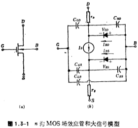
Figure 1.3-1 a is an n-channel MOS FET, and its large signal model is shown in Figure 1.3-1 b. This model is suitable for DC and large signal transient characteristics analysis. In the figure, G, D, and S represent the gate, drain, and source levels of the MOS, respectively, and B represents the substrate. The large-signal model consists of a voltage-controlled current source, two diodes, two resistors and five capacitors. The current source ID simulates the drain-source current of the MOS FET, which is controlled by the port voltage; two diodes D1, D2 Simulate two diodes of substrate-drain and substrate-source respectively; resistance respectively simulate leakage ohmic resistance; capacitance
 the capacitance between the gate source, the gate drain, the gate and the lining gallery,
 、
、 Simulate the Pn junction capacitance between substrate-drain and substrate-source respectively.
If the polarities of the diodes D1 and D2 in Figure 1.3-1b are reversed, it is the large signal model of the P-channel MOS tube.
From the large-signal model, it is easy to get the DC characteristic model and the AC small-signal characteristic model of the MOS tube. We will discuss them separately below.
relevant information
DC characteristic model of MOS field effect tube
Tube capacitance model of MOS field effect tube
AC Small Signal Model and Characteristics of MOS Field Effect Transistor
Contact: Mr. Zou
Contact number: 0755-83888366-8022
Mobile phone: 18123972950
QQ: 2880195519
Contact Address: 5C1, Block CD, Tianji Building, Tianan Digital City, Chegongmiao, Futian District, Shenzhen
Please search WeChat official account: "KIA Semiconductor" or scan the following picture to "Follow" official WeChat official account
Please "follow" the official WeChat account: provide MOS tube technical assistance


