Electronic Technology Forum
The short channel effect characteristics and analysis of MOS field effect transistors
The first-level approximate simulation of MOS FET is given above, and some important relations are derived under approximate conditions. These are undoubtedly very important for the analysis and design of MOS circuits. important. However, with the improvement of the integration and speed of MOS integrated circuits, the device size is getting smaller and smaller, and the channel length is getting shorter and shorter. This produces a short channel effect and lowers the threshold voltage. This requires the threshold voltage relationship Make corrections. In addition, for example, temperature changes cause changes in the performance of MOS devices. In order to improve the accuracy of the design, this section will introduce the secondary effects of some MOS devices and give the corresponding correction formulas.
(1) MOS tube short channel effect
The third section discusses the channel length modulation effect, the channel length modulation parameter λ is (see (1.3-13), (1.3-11) formula)

The above formula shows that the shorter the channel length L, the larger the value of λ. According to typical experimental data, when L is greater than 25 microns, 1 is about 0.01/volt. When the channel length L is less than 25 microns, λ can be expressed as follows:
 < /span>
where L is in micrometers.
After the channel length is shortened, not only the output impedance is reduced, but also the threshold voltage is lowered, and the body effect is weakened. After the channel length is shortened, the total charge Qb of the depletion region that contributes to the threshold voltage will be reduced because the power line that terminates in the depletion layer charge , Partly from the gate voltage, partly from the drain-source voltage, when the channel length is long, the influence of the drain-source voltage power line can be ignored, and it is considered that the charge of the depletion layerQ< /span>b only affects the threshold voltage; MOS tube has short channel effect. After the channel length is shortened, the influence of the drain-source voltage on the charge of the depletion layer cannot be ignored, resulting in the total charge of the depletion region that contributes to the threshold voltageQ b is reduced to lower the threshold voltage.
 < /span>
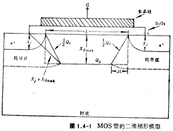
When the channel length is less than 5 microns, the two-dimensional trapezoidal model shown in Figure 1.4-1 can be used to analyze the threshold voltage at this time. In the picture,  is n+ The junction depth of the diffusion zone, L is the channel length,
  is the thickness of the depletion layer.
If the drain-source voltage of the device is assumed to be very small, the width of the depletion layer from source to drain is uniform, and its width is  However, after considering the width of the depletion layer in the source and drain regions, the Depletion layer charge Qˊb is:
 < /span>
and 
From the geometric relationship in Figure 1.4-1:

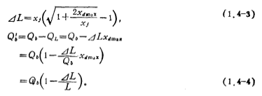
From the above formula we can get:
 < /span>
After considering the depletion layer charge correction, and referring to (1.2-15) and (1.2-18), the body effect factor (substrate bias) γ can be corrected as follows :
Because:
 < /span>
From the above formula:

The corrected body effect factorγˊ is
 < /span>
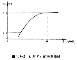
As discussed above, when the channel length L is less than 5 microns, the body effect factor γ decreases , The typical value relationship between L and VT is shown in Figure 1.4-2. The picture is quoted from the reference [2]
 < /span>
When the channel length L is shortened to less than 5 microns, not only should consider the channel length modulation effect, but also The channel length is shortened due to lateral diffusion. At this time, the effective channel length  can be expressed as:
(i) Linear area (1.4-6)
(i) Saturated area (1.4-7)
In the formula Is the diffusion depth, and a is the lateral diffusion correction coefficient.
On the other hand, when we guide the linear region drain-source current ID expression, we assume that The charge Qb of the depletion layer below the channel is constant. In fact, Qb is a function of channel voltage and a variable. Considering that the formula (1.4-6) and Qb are a variable, and [ 11]pp.94~95)
 < /span>
(1.4-8) style VD, VG, VS, VB both Is the voltage at the reference point, a is the correction coefficient for the short channel effect, usually 0.9, when entering the saturation region, the drain voltage  means (see reference [12])

The drain-source current ID in the saturation zone only needs to use (1.4-8) formula (1.4-9) for VD in formula (1.4-8) Just replace it.
In addition, the MOS tube has a short channel effect. . The short channel reduces the drain-source breakdown voltage. The drain-source breakdown voltage of the long-channel MOS FET is mainly the avalanche breakdown of the pn junction, while the drain-source breakdown voltage of the short-channel MOS FET is determined by the punch-through voltage. As a result, the size of the punch-through voltage is related to the channel length, and the shorter the channel length, the lower the punch-through voltage.
relevant information
Short channel MOS field effect transistor model
Contact: Mr. Zou
Contact number: 0755-83888366-8022
Mobile phone: 18123972950
QQ: 2880195519
Contact Address: 5C1, Block CD, Tianji Building, Tianan Digital City, Chegongmiao, Futian District, Shenzhen
Please search WeChat official account: "KIA Semiconductor" or scan the following picture to "Follow" official WeChat official account
Please "follow" the official WeChat account: provide MOS tube technical assistance


