Electronic Technology Forum
AC small-signal model and characteristics of MOS FET
1. AC small signal model of MOSFET
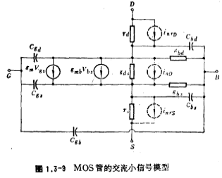
The large-signal model of the MOS FET was discussed earlier. We can derive the AC small-signal model of the MOS FET from the large-signal model of the MOS tube. Figure 1.3-9 is the AC small signal model of the MOS field effect tube evolved from Figure 1.3-1b. The parameters in the figure are defined as follows:
 =The substrate diode D1, D2AC conductance

Because under normal circumstances, the diode D1, D2 is in reverse bias, so < img src="/userfiles/images/2020/12/14/2020121411444912.png" title="image.png" alt="image.png"/> is very small.
 < br/>
 is Positive voltage controlled current source,

 Leak The equivalent noise of the source current (mainly
  noise)

KF=1/f noise figure (typical value is 10-14);
AF=1/f noise figure (typical value is 1.0);
f is the frequency.
In the above model, the noise characteristics of MOS field effect transistors are considered. AC small signal model of MOSFET. The noise of MOS field effect tube includes flicker noise (1/f noise) and 
 thermal noise. When the MOS field effect tube is used in the low frequency range, its
  noise It is often the main noise source, which is closely related to the quality of the gate oxide layer of the MOS FET, which is generally about that of the bipolar transistor. 1/f noise 5 to 10 times of the MOSFET amplifier, so we should pay more attention to the influence of its noise when designing MOS field effect tube amplifiers.
When S and B are short-circuited, the above model can be approximated by the circuit in Figure 1.3-10, and  and the influence of noise. In low frequency applications, the capacitance effect in the figure can also be omitted.
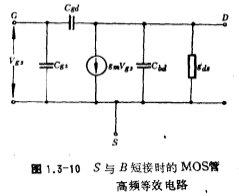
The capacitance in the above model will affect the high frequency characteristics of the MOS FET. To increase the operating frequency of the device, the gate area should be reduced and the channel length of the device should be shortened. In addition, since the effective mobility of electrons in the inversion layer is about 3 times greater than that of holes, the high frequency of the n-channel MOS field effect transistor is better than that of the P-channel MOS field effect transistor.
2. AC small signal characteristics of MOSFET
In the following discussion, the n-channel MOS field effect transistor is still taken as an example, and the result is also applicable to P-channel MOS field effect transistors, as long as VGS, VDS, and VT can be changed accordingly.
(1) Transconductance of MOSFET gm
According to the above definition, transconductance is the rate of change of drain-source current with gate-source voltage when drain-source voltage and substrate-source voltage are constant, and it is used to characterize the input voltage For the control ability of output current, the larger the gm, the stronger the control ability. The gm discussed here refers to the transconductance in the saturation region. gm can be output from the characteristic curve (Figure 1.3-11) to obtain.
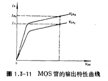
If the channel modulation effect is not considered, then ID The relational expression in the saturation zone is:

according to gm Definition and the above formula, the expression of gm is:

令 
From the above relational formula, gm can be expressed as

It can be seen from the above formula that in order to increase the transconductance, it is required to increase β, that is, increase the channel’s aspect ratio W/L and electron mobility , and reduce the gate oxide thickness tox, and also increase the current ID, but it is most effective to increase the aspect ratio. AC small signal model of MOSFET. Generally speaking, the transconductance of MOS transistors is much lower than that of bipolar transistors.
(2) Substrate transconductancegmb
Substrate transconductancegmb represents the influence of the substrate bias voltage change on the drain-source current of the MOS field effect tube. When the MOS field effect tube is working in the saturation region, ID, V T and other relations (1.3-7), (1.3-9) can be calculated as gmbis:

In the formula
When At this time, the substrate transconductance is very important in AC small signal analysis.
(3) Drain-source output conductance
(i) Output conductance in linear region
According to the definition of output conductance (1.3-29) and ID and VGS, VDS The relational formula (1.3-15) can calculate the output conductance of the MOS field effect tube in the linear region:

When VDS" VGS-VT, the above style can be written As:

Comparing equations (1.3-37) and (1.3-33), we can see that when the MOS FET works in the linear region, its output conductance is the same as the transconductance in the saturation region. Usually on-resistance To represent the output conductance in the linear region, that is

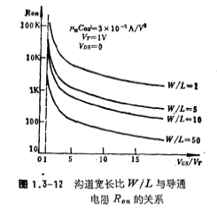
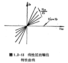
The above formula can also express the on-resistance when the MOS field effect tube is used as an analog switch. Obviously, the larger the channel width-to-length ratio W/L, the larger the VGS, and the smaller the on-resistance. Figure 1.3-12 shows the relationship between the channel width-to-length ratio W/L and the on-resistance. The output characteristic curve of the linear zone is shown in Figure 1.3-13. The reciprocal of the slope of the curve (VDS/ID) means the on-resistance .as VGS-VT gradually increases from zero,
 decrease gradually from infinity.
(Ii) Output conductance in saturation zone
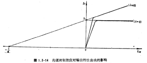
When the MOS FET works in the saturation region, if the modulation effect of the channel length is ignored, the ID will not change with VDS, that is, its Approximately zero, at this time its output resistance tends to infinity. AC small signal model of MOSFET. In fact, due to the influence of the channel modulation effect, the output current increases slightly with the increase of VDS, so that
 increase, output resistance
 become smaller. By (1.3-12)
(1.3-13) The output conductance in the saturation zone can be calculated as:

The relationship between IS and ID in the above formula is:
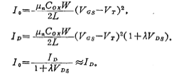
Obviously, the output resistance for:
for:

The relationship between output conductance and λ can be shown in Figure 1.3-14.
From the formula (1.3-44) we can see that the output resistance should be increased. , the channel modulation parameter λ and the working current ID, and λ and ID are inversely proportional to the channel length L, then the output resistance
  is proportional to the square of the channel length L (
 ) . That is, increasing the channel length L can increase the output resistance
 .
.
(4) Noise
Generally speaking, compared with bipolar devices, MOS devices are more noisy. Therefore, in the design of MOS analog circuits, it is necessary to analyze its noise more carefully characteristic.
The noise of MOS devices can be divided into two parts: thermal noise and 1/f noise. The equivalent input noise spectrum is shown in Figure 1.3-15 as shown.
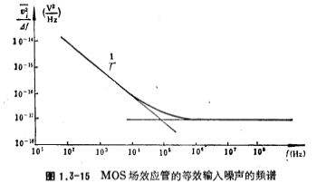
The thermal noise of MOS devices is mainly produced by the limited channel resistance, and its equivalent input thermal noise voltage is

where gm is the transconductance of the device.
As can be seen from the above formula, thermal noise is related to temperature, device size (channel width-to-length ratio) and its bias current. For n-channel MOS devices, its operating current is 50 microamperes, the width and length of the channel WL==100×10 microns2 and the oxide layer thickness< img src="/userfiles/images/2020/12/14/2020121415031653.png" title="image.png" alt="image.png"/>At 1200 hours,The thermal noise voltage is 10 nanovolts/(Hz)1/2.
The other part is the 1/f noise generated by the interface state of silicon and silicon dioxide, and its value is:

In the formula, a is approximately 1. The typical value of KF is 3×1024 (volt 2 ● method)/Hz. For n-channel MOS devices, its operating current is 50 microampere, channel WL is 100×10 micrometers, and when the frequency is 1 kilohertz, its The 1/f noise voltage is about 100 nanovolts/(Hz) 1/2.
Contact: Mr. Zou
Contact number: 0755-83888366-8022
Mobile phone: 18123972950
QQ: 2880195519
Contact Address: 5C1, Block CD, Tianji Building, Tianan Digital City, Chegongmiao, Futian District, Shenzhen
Please search WeChat official account: "KIA Semiconductor" or scan the following picture to "Follow" official WeChat official account
Please "follow" the official WeChat account: provide MOS tube technical assistance


