Electronic Technology Forum
The characteristics and detailed analysis of the capacitance model of MOS field effect tube
The five capacitors in the MOS tube large-signal model (see Figure 1.3-1b) and
and for
for junction barrier capacitance,
 、
、 and
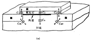
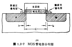
and For the gate capacitance, the distribution of these MOS capacitance models is shown in Figure 1.3-7a and b. The following two types are used to discuss their models.
1, pn junction potential will be capacitance and
and

where is the junction capacitance per unit bottom area at zero bias voltage, AD is the area of the drain area of the MOSFET, AS is the area of the source area of the MOSFET, and m is the gradient factor of the bottom surface capacitance (generally taken
 ),
), is the contact potential difference of the pn junction between the drain-source region and the substrate (usually 0.8 volts),
 is the junction capacitance per unit circumference at the zero bias voltage, PD is the circumference of the drain region, PS is the circumference of the source region, and mjsw is the gradient factor of the side capacitance (generally taken
 ):CjandCjswis the model parameter to be determined.
2. Grid-view capacitance and
and
Figure 1.3-7a and b respectively show the five capacitance distributions of the MOS tube and the cross-sectional structure of the MOS tube. In the figure, Is is the overlap length of the gate oxide layer and the source region, the MOS capacitance model, and ID is the gate oxide layer and the cross-sectional structure of the MOS tube. The overlap length of the drain region, is the gate-source overlap capacitance,
 is the gate-drain overlap capacitance, C2 is the gate oxide capacitance, and C4 is the gate-substrate capacitance.


When the MOSFET is in the off state, that is, the inversion layer channel between the drain and the source is not formed, the gate capacitance can be expressed as:

in , C4 is larger at the end, so
 。
。
When the MOSFET is in the linear region, an inversion layer channel is formed between the drain and the source, and a thicker depletion layer is formed between the channel and the substrate, forming a smaller depletion layer capacitance C4, at this time the gate capacitance Can be expressed as:

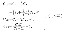
When the MOSFET is in the saturation region, the drain terminal is pinched off and the channel length is shortened. MOS capacitor model. Considering the channel charge distribution, it is equivalent to increasing CGS and decreasing CGD. At this time, the gate capacitance can be approximately expressed as:

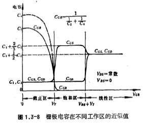
The approximate values of the above-mentioned shed capacitors in different working areas can be shown in Figure 1.3-8.

The five capacitors of the MOS tube are discussed above. These capacitors determine the AC characteristics and transient characteristics of the MOS tube.
Contact: Mr. Zou
Contact number: 0755-83888366-8022
Mobile phone: 18123972950
QQ: 2880195519
Contact Address: 5C1, Block CD, Tianji Building, Tianan Digital City, Chegongmiao, Futian District, Shenzhen
Please search WeChat official account: "KIA Semiconductor" or scan the following picture to "Follow" official WeChat official account
Please "follow" the official WeChat account: provide MOS tube technical assistance


