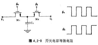
MOS switched capacitor, equivalent resistance of MOS switched capacitor, equivalent resistance circuit and calculation formula of MOS switched capacitor In recent years, in MOS analog integrated circu
MOS switched capacitor, equivalent resistance of MOS switched capacitor, equivalent resistance circuit and calculation formula of MOS switched capacitor In recent years, in MOS analog integrated circu

In MOS integrated circuits, in addition to MOS field effect transistors, it is often necessary to fabricate resistors, capacitors and other components on the same chip, and sometimes requires higher m
In MOS integrated circuits, in addition to MOS field effect transistors, it is often necessary to fabricate resistors, capacitors and other components on the same chip, and sometimes requires higher m
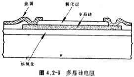
The manufacturing process of MOS tube resistors, in MOS integrated circuits, in addition to MOS field effect transistors, it is often necessary to fabricate resistors, capacitors and other components
The manufacturing process of MOS tube resistors, in MOS integrated circuits, in addition to MOS field effect transistors, it is often necessary to fabricate resistors, capacitors and other components

Silicon gate CMOS process, silicon gate CMOS process steps, although the aluminum gate CMOS process is relatively mature and stable, but due to the large gate-drain and gate-source overlapping parasit
Silicon gate CMOS process, silicon gate CMOS process steps, although the aluminum gate CMOS process is relatively mature and stable, but due to the large gate-drain and gate-source overlapping parasit
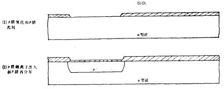
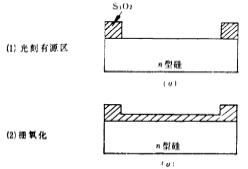
CMOS aluminum gate-silicon gate, CMOS aluminum gate-silicon gate process, 1. P-well oxidation and p-well photolithography, thermally grow a layer of SiO2 on the n-type silicon wafer, as a masking laye
CMOS aluminum gate-silicon gate, CMOS aluminum gate-silicon gate process, 1. P-well oxidation and p-well photolithography, thermally grow a layer of SiO2 on the n-type silicon wafer, as a masking laye
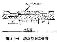
The MOS channel stop ring, MOS and other planar isolation processes, should be naturally isolated between the field effect transistors in the CMOS integrated circuit, as shown in Figure 4.1-4.
The MOS channel stop ring, MOS and other planar isolation processes, should be naturally isolated between the field effect transistors in the CMOS integrated circuit, as shown in Figure 4.1-4.
CMOS process aluminum gate and silicon gate process. In addition to aluminum, polysilicon can also be used as the gate material in MOS field effect transistors. As long as the polysilicon is doped wit
CMOS process aluminum gate and silicon gate process. In addition to aluminum, polysilicon can also be used as the gate material in MOS field effect transistors. As long as the polysilicon is doped wit

The CMOS circuit is composed of two types of MOS field effect transistors, p-channel and n-channel. We can fabricate the p-channel MOS field effect transistor on the n-type silicon wafer substrate, an
The CMOS circuit is composed of two types of MOS field effect transistors, p-channel and n-channel. We can fabricate the p-channel MOS field effect transistor on the n-type silicon wafer substrate, an
MOS op amp computer SPICE program running assistance, detailed explanation of SPICE program running instructions, operation steps for users to run SPICE on the VAX-11/750 computer of the Department of
MOS op amp computer SPICE program running assistance, detailed explanation of SPICE program running instructions, operation steps for users to run SPICE on the VAX-11/750 computer of the Department of
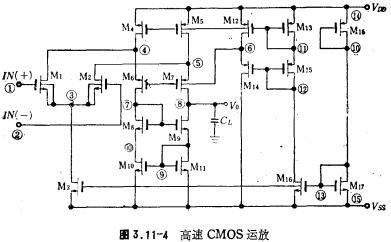
CMOS operational amplifier analysis, CMOS operational amplifier DC work-DC conversion-AC small signal-transient characteristics analysis, for general operational amplifier, computer-aided simulation m
CMOS operational amplifier analysis, CMOS operational amplifier DC work-DC conversion-AC small signal-transient characteristics analysis, for general operational amplifier, computer-aided simulation m


5C1, CD Block, Tianji Building, Tianan Digital City, Futian District, Shenzhen

KIA-The Public