Electronic Technology Forum
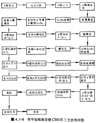
Detailed explanation of typical process distribution flow of CMOS aluminum gate-silicon gate and other planar isolation
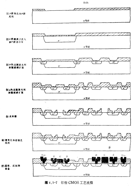
The flow of aluminum gate CMOS is shown in Figure 4.1-7. A brief description is as follows:

1. P-well oxidation and p-well lithography
A layer of SiO2 is thermally grown on the n-type silicon wafer as a masking layer for P-well ion implantation. The thickness of the oxide layer is determined by ion implantation energy, dose, and p-well redistribution temperature and time. Generally, it is required to be above 5000 angstroms. Then photolithography is performed to etch away the oxide layer in the P-well region.
2. P-trap boron ion implantation and redistribution
The P-well is the substrate of the n-channel MOS tube in the CMOS circuit. The impurity concentration on the surface of the P-well directly affects the threshold voltage of the n-channel MOS field effect transistor. Therefore, the energy and dose of the P-well ion implantation must be strictly controlled. The redistribution conditions of the P-well, because the impurity concentration of the P-well is relatively light (the surface concentration is about 1015/cm3, and the concentration becomes lighter as the diffusion depth increases), the pn between the n-channel drain-source region and the P-well The width of the junction depletion layer is relatively wide, so the depth of the P well cannot be too shallow to prevent punch-through between the n-channel drain-source region and the n-silicon substrate, and to prevent the β of the parasitic npn bipolar transistor from being too large. Generally, the depth of the P trap is about 8-10 microns, the redistribution temperature is 1200°C, and the time is about 10 hours.
While the P-well is redistributed, thermal oxidation is also performed to serve as a mask for the next p+ and n- diffusion. In the thermal oxidation process, many B+ ions will inevitably go to SiO2, so the dose of ion implantation must be appropriately large. Quantitative analysis can be calculated by computer process simulation, generally taking the order of 1013/cm2.
3. P-channel drain-source lithography and drain-source boron diffusion
At the same time as the P-channel drain-source lithography, the P+ channel stop ring around the NMOS tube is carved out at the same time, so as to perform P+ boron diffusion together. Thermal oxidation is performed while boron diffuses to serve as a protective layer on the p+ region and a mask for the next n+ diffusion.

4. N-channel drain-source lithography and drain-source phosphor diffusion
Simultaneously with the n-channel drain-source lithography, the n+ channel cut-off ring around the PMOS transistor is carved out at the same time, so as to carry out n+ phosphorus diffusion together. Thermal oxidation is also performed while phosphorous is diffused to serve as a protective layer on the n+ region.
5. Lithography grid
When carving out the gate area of the MOS tube, the lead hole is also carved out to facilitate the subsequent corrosion of the lead hole.
6. Gate oxidation and contact hole lithography
A clean oxidation process is used to grow a high-quality thin gate oxide layer on the silicon wafer, and then lead hole photolithography is performed.
7. Steamed aluminum reverse engraving and alloy
Contact: Mr. Zou
Contact number: 0755-83888366-8022
Mobile phone: 18123972950
QQ: 2880195519
Contact Address: 5C1, Block CD, Tianji Building, Tianan Digital City, Chegongmiao, Futian District, Shenzhen
Please search WeChat official account: "KIA Semiconductor" or scan the following picture to "Follow" official WeChat official account
Please "follow" the official WeChat account: provide MOS tube technical assistance


