Electronic Technology Forum
CMOS process aluminum gate and silicon gate process steps and layout design examples analysis
1. CMOS process aluminum gate
In addition to aluminum, polysilicon can also be used as the gate material in the MOS field effect tube, as long as the polysilicon is doped with certain impurities to make it more conductive.

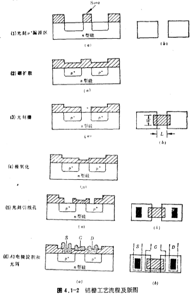
In the aluminum gate CMOS process, aluminum is used as the gate material. Since the aluminum material is not resistant to high temperatures, a high-temperature drain-source diffusion process must be performed first, and finally the aluminum gate electrode is deposited. For example, to make a p-channel MOS tube, the specific process steps are: first lithographically etch the P-channel drain-source region, perform boron diffusion to form the drain and source of the p-channel MOS tube; The oxide layer is subjected to gate oxidation and photoetching of lead holes; finally, while the aluminum connection is formed, the aluminum gate electrode is covered on the gate oxide layer.
The process steps are:
(1) Photolithography p+ drain-source area;
(2) Boron diffusion;
(3) Lithography grid;
(4) Gate oxidation;
(5) Lithography lead hole;
(6) Aluminum electrode deposition and photolithography.
As shown in Figure 4.1-2a. Figure 4.1-2b shows the corresponding layout of the p-channel MOS tube.

2. CMOS process silicon gate
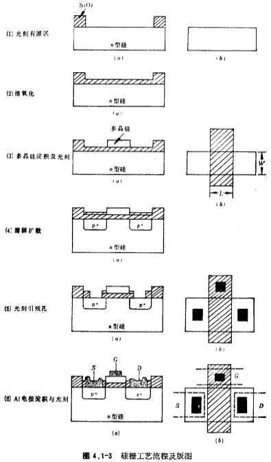
In the silicon gate CMOS process, polysilicon is used as the gate material. Because polysilicon is resistant to high temperatures, it is possible to make polysilicon gates in the process steps first, and then perform high-temperature drain-source diffusion, as shown in Figure 4.1-3a, and Figure 4.1-3b is the corresponding layout of the p-channel MOS tube.
In the aluminum shed process, the mask design of the photoetched gate and the aluminum gate electrode must overlap with the drain-source region to ensure that the channel region between the drain and source of the MOS tube is indeed controlled by the gate voltage. The amount of overlap depends on the registration accuracy that can be achieved by lithography. Therefore, the MOS tube made by the aluminum gate process has large gate-source and shed-drain parasitic capacitances.
In the silicon gate process, the polysilicon gate electrode is made first, and then the silicon gate electrode is used as a mask for drain-source diffusion. This process realizes the self-alignment of the gate electrode and the drain-source region, that is, eliminates the gate electrode and The overlapping parasitic capacitance between the drain and source regions greatly increases the speed of the circuit. Of course, due to the lateral diffusion during the drain-source diffusion, there is still an overlap between the gate-source and the gate-drain, but compared to the aluminum gate process, the overlap is much smaller.
In addition, in the silicon gate process, polysilicon can be used as a circuit connection in addition to the gate electrode. In this way, it is equivalent to a natural double-layer wiring, which facilitates circuit layout and saves chip area.
In logic circuits, aluminum gate and silicon gate CMOS have formed two major product series. Aluminum gate CMOS products have low speed, but the process is relatively simple, so the price is cheap. The silicon gate CMOS has a high speed, but the process is more complicated and the price is more expensive. In CMOS analog circuits, more aluminum gates were used in the early stage, but now the use of silicon gates is gradually increasing.
In large-scale integrated circuits, there are many and long connections. Polysilicon connections are used. The resistance of the square is large, which is not conducive to the increase in speed. Use refractory metals such as buttons or silicides such as tungsten silicide and titanium silicide as the gate. The circuit of polar materials has been developed.
Contact: Mr. Zou
Contact number: 0755-83888366-8022
Mobile phone: 18123972950
QQ: 2880195519
Contact Address: 5C1, Block CD, Tianji Building, Tianan Digital City, Chegongmiao, Futian District, Shenzhen
Please search WeChat official account: "KIA Semiconductor" or scan the following picture to "Follow" official WeChat official account
Please "follow" the official WeChat account: provide MOS tube technical assistance


