Electronic Technology Forum
Process manufacturing method and characteristic analysis of MOS tube capacitor
(1) Capacitance
In MOS integrated circuits, in addition to MOS field effect transistors, resistors, capacitors and other components are often made on the same chip, and sometimes higher matching accuracy is required. The following describes the manufacturing methods and characteristics of several passive components.
In the MOS analog integrated circuit, the capacitor is one of the indispensable basic components, and its performance and accuracy directly affect the performance of the circuit. MOS tube capacitance. Because MOS capacitors implemented in MOS technology have better matching accuracy than resistors, generally about 0.1% to 5%, capacitors are often used instead of resistor networks in integrated circuits such as D/A, A/D, and switched capacitor circuits. .
Now the manufacturing methods and performance of several MOS capacitors in MOS integrated circuits are introduced as follows.
1. Aluminum-gate oxide-drain-source diffusion area capacitance in aluminum gate process
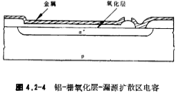
In the standard aluminum gate process, an aluminum-gate oxide-drain-source diffusion capacitor is provided. The capacitor structure is shown in Figure 4.2-4.

The aluminum layer serves as the upper electrode, the drain-source region n+ or p+ serves as the lower electrode, and the gate oxide layer serves as the capacitor medium. When the thickness of the gate oxide layer is 1000 angstroms, the capacitance value per unit area is image.png method/cm3. The capacitance area is determined by the gate lithography or aluminum lithography. The voltage coefficient of this capacitor is about 10~100 million One part/volt, the temperature coefficient is about 10-20 millionth/℃, which are relatively low. MOS tube capacitance. However, it can be seen from Figure 4.2-4 that the bottom electrode of the capacitor and the substrate form a reverse pn junction capacitance, forming a parasitic capacitance; the upper electrode (aluminum layer) of the capacitor also forms a parasitic capacitance with the substrate, and the field oxide layer is usually thicker. Therefore, the parasitic capacitance is relatively small. If the aluminum-gate oxide-drain-source diffusion capacitor is used in the circuit design, the influence of the parasitic capacitance of the lower electrode of this capacitor on the circuit should be considered.
2. The capacitance between polysilicon and heavily doped substrate in the silicon gate process
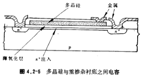
In the silicon canopy process, due to its self-aligning characteristics, the overlap capacitance between the polysilicon and the drain source is very small, usually negligible, and only the MOS capacitance between the polysilicon and the low-doping concentration substrate is considered. This MOS capacitor The voltage coefficient of is very large, usually can not be used. MOS tube capacitance. To this end, an ion implantation plate needs to be added, and the implantation concentration is 1013~1014/cm1, and a capacitance between polysilicon and heavily doped substrate is obtained. The dielectric is also a gate oxide layer. The capacitance structure is shown in Figure 4.2-5. When the thickness of the gate oxide layer is 1000 angstroms, the capacitance per unit area is method/cm2. Obviously, the upper electrode and the lower electrode of this capacitor also have parasitic capacitance.

3. Aluminum-polysilicon capacitors in silicon gate technology
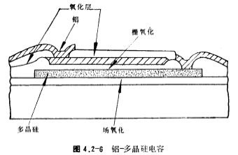
Before the aluminum vaporization process of the silicon gate process, the thick oxide layer on the polysilicon is etched by photolithography, and then a thin oxide layer (made at the same time as the gate oxide layer) is thermally grown on the polysilicon, and then aluminum is evaporated, and finally formed The structure of an aluminum-oxide-polysilicon capacitor is shown in Figure 4.2-6. MOS tube capacitance. The bottom of the polysilicon is a thick field oxide layer (about 1 micron), so the parasitic capacitance between the lower electrode of the capacitor and the substrate is very small, usually 10% of the capacitance of the capacitor C, and the parasitic between the upper electrode of the capacitor and the substrate The capacitance is smaller, generally 0.1% to 5% of the capacitance of the capacitor C.

4. Double-layer polycrystalline capacitors in silicon gate technology
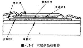
The structure of the double-layer polysilicon capacitor in the silicon gate process is shown in Figure 4.2-7. Between the two layers of polysilicon is a thin oxide layer. This oxide layer is usually formed at the same time as the gate oxide layer, and its thickness is 600~1000 angstroms. MOS tube capacitance. As can be seen from Figure 4.2-7, this capacitor is the same as the aluminum-polysilicon capacitor with very small parasitic capacitance. Because double-layer polysilicon capacitors have the advantages of stable performance and small parasitic capacitance, they are usually used as capacitors in switched capacitor circuits, A/D, D/A, and other integrated circuits.
Contact: Mr. Zou
Contact number: 0755-83888366-8022
Mobile phone: 18123972950
QQ: 2880195519
Contact Address: 5C1, Block CD, Tianji Building, Tianan Digital City, Chegongmiao, Futian District, Shenzhen
Please search WeChat official account: "KIA Semiconductor" or scan the following picture to "Follow" official WeChat official account
Please "follow" the official WeChat account: provide MOS tube technical assistance


