Electronic Technology Forum
CMOS operational amplifier DC work-DC conversion-AC small signal-transient characteristics analysis
For general operational amplifiers, computer-aided simulation mainly understands the following operating characteristics.
1. Analysis of DC operating point
The purpose of this analysis is to simulate the DC working state of the op amp and confirm whether the working points of the circuit meet the design requirements. Usually, the input terminals are all grounded. At this time, the voltage appearing at the output terminal is caused by the offset of the op amp. DC analysis is available. The OP statement is complete.
2. DC conversion standby
Use a .DC statement or a TRAN statement (when using .TRAN, add a pulse source with a long enough rise time or a piecewise linear source at the input) to scan the entire voltage range to determine the dynamic range and common mode of the op amp Enter the range.
3. AC small signal analysis
The AC small signal analysis mainly completes the frequency domain analysis of the operational amplifier. Generally, add a small AC signal at the input (its value is small enough so that the output does not enter the saturation zone), and print the amplitude and phase of the output voltage to obtain the amplitude-frequency (referred to as amplitude-frequency) characteristics of the operational amplifier and Phase frequency (referred to as phase frequency) characteristics. Use .AC and .PRINT statements to complete this analysis.
4. Transient analysis
Short-circuit the inverting input end of the op amp and the output end to form a follower form. Add a pulse source or a piecewise linear source with a sufficiently short rise time to the non-inverting input terminal and print the output voltage to obtain transient response parameters such as slew rate and settling time. Transient analysis is done by .TRAN and .PRINT.
5. Common mode rejection and power rejection characteristics
The measurement of common mode rejection ratio and power supply rejection ratio is part of AC small signal analysis. Add differential mode and common mode small signals at the input, and divide the differential mode magnification by the common mode magnification, which is the common mode rejection ratio (CMRR). If the input terminal is grounded, and a small AC signal is superimposed on the positive or negative power supply, the amplification factor obtained at the output terminal is divided by the differential mode amplification factor, which is the power supply rejection ratio (SPRR) of the positive or negative power supply. Unfortunately, SPICE does not have the function of dividing the output result. Therefore, if you need to draw CMRR and SPRR curves, users can only process the output results themselves.
Let's briefly explain the simulation of CMOS op amp with two examples.
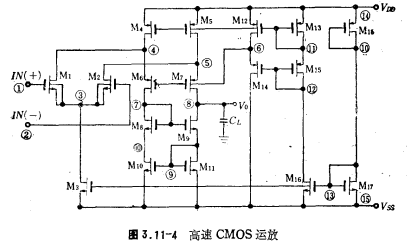
[Example 1] Figure 3.11-4 shows a high-speed CMOS op amp with a cascode structure. The tube aspect ratios in the figure are listed in Table 3.11-2.
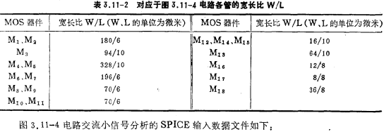
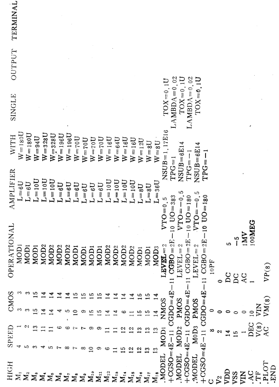
SPICE stipulates that the ground node number is zero. In the above model statement, the parameter "LAMBDA" reflects the channel modulation effect of the MOS device. Usually, the value is given empirically: when the channel length is about 10 microns, the LAMBDA value is 0.02, and when the channel length is less than 6 microns and greater than 3 microns, the value is 0.03. The default value of LAMDA is zero. In the file, .AC specifies that when a small signal of 1 millivolt is input, the bridge starts from 1 Hz to 100 MHz and divides the bridge at 10 points per decade.
The DC operating point analysis results (the voltage of each node) automatically performed by SPICE before AC analysis are as follows:
(1) 0.0000 (2) 0.0000 (3) -1.5451 (4) 3.3680 (5) 3.3680
(6) 1.6587 (7)-0.0049 (8)-0.0049 (9)-3.1134 (10)-3.1134
(11) 2.9756 (12) -0.7417 (13) -1.8948 (14) 5.000 (15)-5.0000
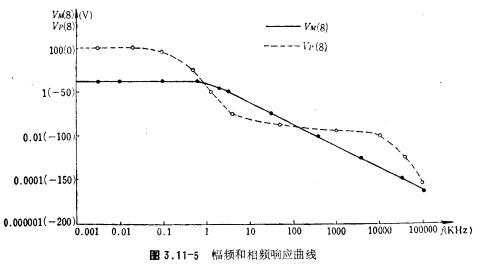
It can be seen that the voltage of the output node 8 is close to zero, that is, the circuit offset voltage is very small. The phase-frequency response and amplitude-frequency response curves drawn according to the requirements of the .PLOT statement are shown in Figure 3.11-5. The unity gain frequency corresponding to the curve is about 3.2 MHz, and the open loop gain is 3.23×10³ times.
The input file for transient analysis of the op amp is as follows:
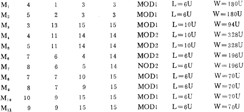
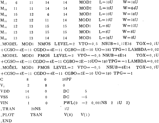
SPICE does not allow zero-value resistance, therefore, short circuits are generally represented by zero-value independent sources. For example, the voltage source V2 in the above file means that nodes 2 and 8 are short-circuited. The input voltage source VIN uses a piecewise linear source PWL to describe a pulse signal that jumps from 0 to 2 volts and has a rise time of 0.001 nanoseconds. It starts from 0 to 1 microsecond, and analyzes one point every 20 nanoseconds. The output curve is shown in Figure 3.11-6.
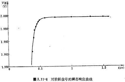
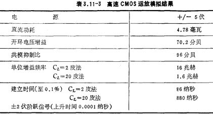
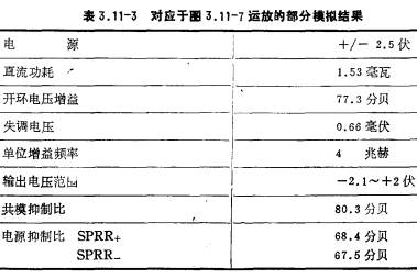
It can be seen from the curve that the settling time of the op amp is about 430 nanoseconds. The simulation results of some other parameters of the op amp are listed in Table 3.11-3
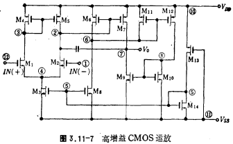
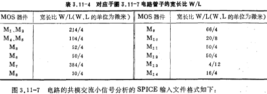
[Example 2] Figure 3.11-7 shows a high-gain CMOS operational amplifier used in switched capacitor filter 6517. The width-to-length ratio of each tube in the circuit is listed in Table 3.11-4.
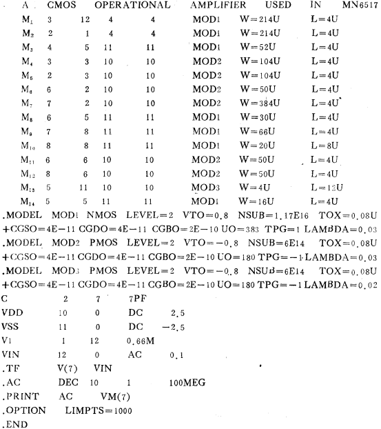
The voltage source V1 in the above input data file is the offset voltage applied to the input terminal of the operational amplifier. In the design of the op amp, due to the approximate estimation of the parameters, the simulation result of the DC operating point of the op amp often shows a large offset voltage, which makes the op amp in an abnormal working state, in order to continue to simulate the steady-state and transient characteristics of the op amp , "Usually two methods are used. One is to add a proper offset voltage source to the input to just offset the offset of the circuit itself and restore the circuit to its normal working state, that is, when the input is zero, the output is also zero. One method is to add an appropriate feedback resistor to form a negative feedback amplifier, first analyze the various characteristics of the negative feedback amplifier, and then convert it to the open loop parameters of the operational amplifier.
It can be seen from the simulation output result that the common-mode amplification of the operational amplifier is 0.7078 times. Connect the negative input terminal in the above file to ground, and connect the positive input terminal to a 1 millivolt AC small signal, and the output is the differential mode frequency response characteristic of the op amp. According to the simulation results, the open-loop magnification is 7338 times. Thus the common mode rejection ratio is

The following input file is the power supply suppression capability of the analog op amp.
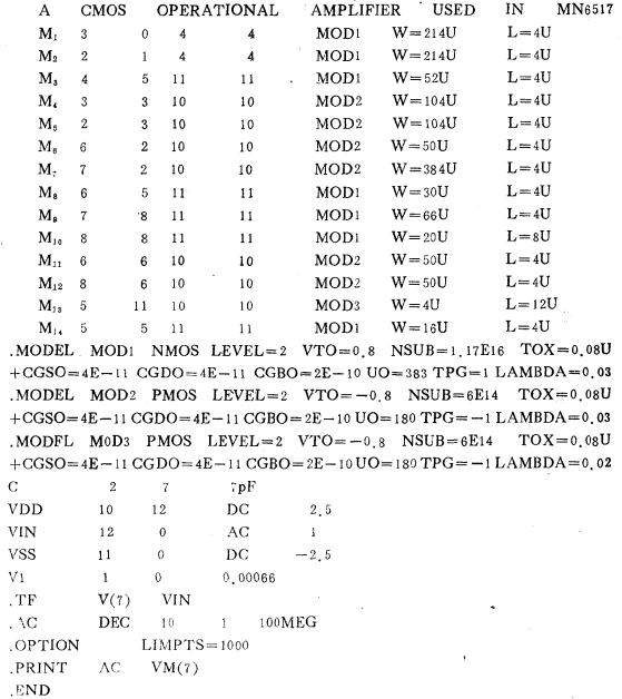
An offset voltage is connected between the two input terminals of the operational amplifier, and then grounded, and an AC small signal is superimposed on the DC power supply on the positive power supply node 10, and the response of the output terminal 7 to the input is analyzed and printed.
The simulation results show that the amplification of the small signal superimposed on the positive power supply is 2.8 times, and the power supply rejection ratio of the op amp to the positive power supply is obtained as

The power supply rejection ratio of the op amp to the negative power supply can be obtained in the same way. Some simulation results of the op amp are listed in Table 3.11-3.
Contact: Mr. Zou
Contact number: 0755-83888366-8022
Mobile phone: 18123972950
QQ: 2880195519
Contact Address: 5C1, Block CD, Tianji Building, Tianan Digital City, Chegongmiao, Futian District, Shenzhen
Please search WeChat official account: "KIA Semiconductor" or scan the following picture to "Follow" official WeChat official account
Please "follow" the official WeChat account: provide MOS tube technical assistance


