Electronic Technology Forum
Technical analysis of planar isolation technology such as MOS tube stop ring and local oxidation
1. MOS channel stop ring
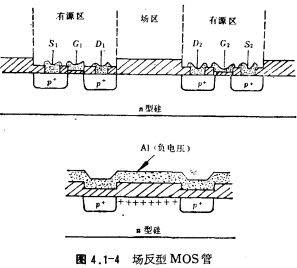
The field effect transistors in the CMOS integrated circuit should be naturally isolated, as shown in Figure 4.1-4. The drain source of tube 1 is reverse biased to the substrate, and the drain source of tube 2 is also reverse biased to the substrate, so the drain sources of the two tubes are isolated from each other. But in the actual circuit, there are parasitic MOS field effect transistors between the tubes, which are called field inversion MOS transistors. As shown in Figure 4.1-4, the area between the two tubes is called the field area. When there is a negatively charged aluminum strip across the field area, as long as the negative voltage is high enough, the surface of the silicon in the field area will also be inverted, so that The field inversion MOS tube is turned on, and the voltage on the aluminum bar when the field inversion MOS tube starts to be turned on is called the field turn-on voltage VTF. To obtain good isolation characteristics between the tubes, the field turn-on voltage is required to be sufficient, high enough, and at least greater than the power supply voltage used by the circuit.

The size of the field turn-on voltage is related to the thickness of the oxide layer in the field region and the doping concentration of the silicon substrate. The thicker the oxide layer, the greater the substrate concentration.
Higher, the higher the field turn-on voltage. For this reason, planar isolation methods such as channel stop ring or local oxidation can be used to improve the VTF, and the isolation between the tubes is now.

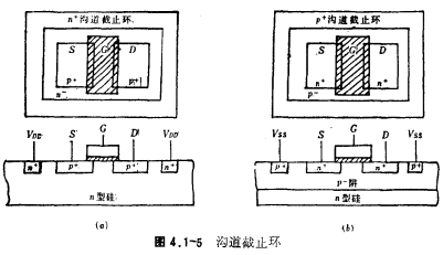
The so-called channel stop ring is to make a circle of n+ ring on the surrounding substrate of the p-channel MOS tube to prevent the n-substrate area from being inverted into p-type and turning on the field inversion MOS tube, as shown in Figure 4.1-5a As shown, at the same time, a p+ ring is made on the surrounding substrate (p well) of the n-channel MOS tube to prevent the p-substrate region from being inverted into n-type, and the n-channel field inversion MOS tube is turned on, such as As shown in Figure 4.1-5b, in a CMOS integrated circuit, the n+ channel stop ring of the PMOS tube can be diffused simultaneously with the drain-source phosphorus diffusion of the NMOS tube, and the p+ channel stop ring around the NMOS tube can be reversed with the drain source of the PMOS tube Diffusion is carried out at the same time, so its manufacturing process is relatively simple; because the cut-off ring diffuses together with the drain source, its concentration is higher, so a higher field turn-on voltage can be obtained. The disadvantage is that the cut-off ring occupies an area Larger and not highly integrated.
The channel stop ring increases the field turn-on voltage VTF by increasing the substrate impurity concentration. At the same time, it can also increase the field turn-on voltage by increasing the thickness of the oxide layer. However, if the oxide layer is thick, there will be a high step between the field area and the active area, and when the aluminum bar crosses the step, the phenomenon of aluminum disconnection will occur. In order to overcome this kind of broken aluminum field image, a plane isolation process such as local oxidation has been developed.
2. Plane isolation technology such as MOS
The plane isolation process such as partial oxidation is shown in Figure 4.1-6. Its process is to cover the active area with Si3N4 to conceal the growth of thick oxide and form a thicker field oxide layer in the field area. Since the growth of SiO2 is a chemical reaction between oxygen and silicon, a certain amount of silicon is inevitably consumed during the oxidation process. Therefore, about 40% of the thickness of the field oxide layer is buried below the silicon surface of the active area, which reduces the field area and the amount of silicon. The height of the steps between the source regions has the effect of iso-plane isolation. The process steps are: (1) initial oxidation; (2) deposition of Si3N4; (3) photolithography field area; (4) field oxidation; (5) removal of Si3N4.
Since the ion implantation technology is available, Si3N4 can be used as a mask for field implantation. For example, phosphorus is implanted in the field region of a p-channel MOS tube, and boron is implanted in the field region of an n-channel MOS tube to increase the field region lining. The bottom doping concentration further increases the field turn-on voltage VTF.
Contact: Mr. Zou
Contact number: 0755-83888366-8022
Mobile phone: 18123972950
QQ: 2880195519
Contact Address: 5C1, Block CD, Tianji Building, Tianan Digital City, Chegongmiao, Futian District, Shenzhen
Please search WeChat official account: "KIA Semiconductor" or scan the following picture to "Follow" official WeChat official account
Please "follow" the official WeChat account: provide MOS tube technical assistance


