Electronic Technology Forum
Silicon gate CMOS process flow diagram and isoplanar isolation silicon gate CMOS process steps
1. Block diagram of silicon gate CMOS process flow
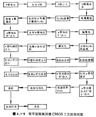
Although the aluminum gate CMOS process is relatively mature and stable, the circuit speed is relatively slow due to the large gate-drain and gate-source overlapping parasitic capacitance. In addition, the n+ and p+ channel stop rings occupy a large area. The level of integration is not high, so the iso-planar isolation silicon gate CMOS process is developed on the basis of the iso-planar isolation n-channel silicon canopy process. Although this process has a longer process flow, it reduces the area of the CMOS circuit, improves the speed performance of the circuit, and the layout design is simple and regular, and is suitable for computer-aided plate making. Therefore, it has become the main process in the current MOS process.
Figure 4.1-8 shows the process flow diagram of iso-plane isolation silicon shed CMOS.

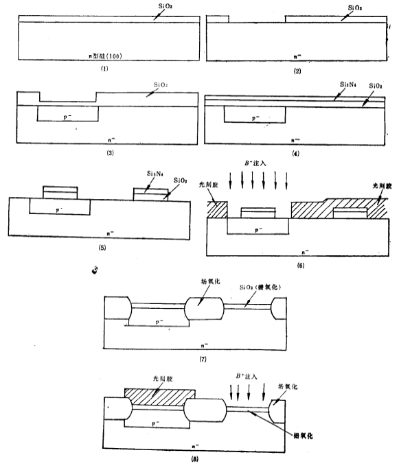
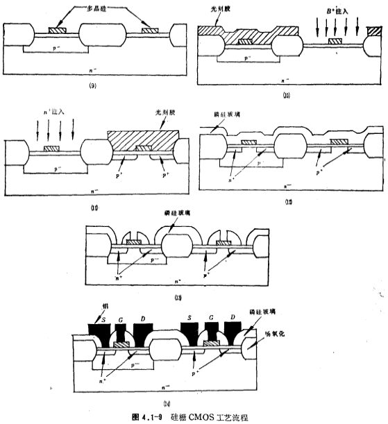
Figure 4.1-9 shows the process flow of iso-plane isolation silicon gate CMOS.


2. Process steps
Combined with Figure 4.1-8 and Figure 4.1-9, we briefly introduce the process flow steps of silicon gate CMOS;
(1) Pre-oxidation
The first step of thermal oxidation is performed on n-type (100) silicon wafers as a mask for P-well implantation and redistribution.
(2) P-well lithography
(3) P-trap boron ion implantation and P-trap redistribution
The P-well implant dose has a direct impact on the threshold voltage image.png of the n-channel MOS tube. The implant dose must be determined according to the circuit's requirements for image.png, which is generally about 1013/cm2.
(4) Oxidation of bottom oxygen and deposition of Si3N4
First remove the pre-oxidation layer, and then perform bottom oxidation and Si3N4 deposition as a mask for field oxidation.
(5) Lithography field area
Where field oxidation is needed, Si3N4 is removed by photolithography and plasma etching.
(6) n-channel field injection lithography
In order to increase the field turn-on voltage VTF of the n-channel field region, the n-channel field region must be implanted with boron. Since the active region has been masked by Si3N4, boron ions will not be implanted, so the field implantation lithography and P-well plate shape The same, as long as the area outside the P well is masked with photoresist. Silicon gate CMOS process. The dose of n-channel field implantation is determined by VTF, which is generally on the order of 1013/cm. The implantation energy should be appropriate. If the energy is too low, it will easily enter the field oxide layer during field oxidation; if the energy is too high, it will pass through Si3N4 to the active area. So as to affect the MOS field effect tube After the field injection, the glue is removed. After the glue is removed, the photolithography pattern is no longer retained.
(7) Field oxidation and Si3N4 removal
Through a long time of wet oxygen oxidation, an oxide layer of about 1 micron is grown in the field area to increase the field turn-on voltage. After the field oxidation is completed, Si3N4 is removed with hot phosphoric acid.
(8) Shed oxidation and VTF adjustment B+ injection
Remove the bottom oxygen under Si3N4, perform clean oxidation again, and grow a thin gate oxidation sense on the gate area of the MOS tube; then perform adjustment photolithography. Silicon gate CMOS process.
Adjust the photolithography, as long as the n-channel MOS tube area is masked with photoresist, so the reverse version of the P well can be used. This photolithography does not need to be etched, and the pattern will not be retained after de-glue.
VTF adjustment is achieved by ion implantation of boron. The implantation dose is about 1011/cm2, and the energy can be lower as long as it can pass through the gate oxide layer.
(9) Polysilicon deposition, polysilicon doping and polysilicon photolithography
Use low pressure chemical vapor deposition (LPCVD) method to deposit a layer of polysilicon on the surface of the entire silicon wafer, and then carry out phosphorus diffusion to make the R□≈30 ohm/square of the polysilicon, and then carry out polysilicon photolithography to connect the MOS field effect transistor gate The polysilicon on the area and the polysilicon used for connection are retained, and the polysilicon in other places is removed by plasma etching.
(10) P+ area photolithography, boron implantation in P+ area
In order to implant boron in the P+ region (P channel drain source region and P+ ring in the P well), the n+ region must be masked and long with photoresist. As for the field region, there is a thick field oxide layer. The track area is masked by polysilicon, so there is no need to consider any additional masking. The P+ area can be implanted with boron ion without etching during photolithography. In order to reduce the resistance of the drain-source area of the P-channel, the injection dose should be slightly larger, generally 1014~1016/cm2. After the implantation is completed, the glue will be removed and the glue will be removed. The post graphics are not retained.
(11) Lithography of n+ area, phosphorus (or arsenic) implantation in n+ area
When performing photolithography of the n+ region (n channel drain source region and n+ electrode in the n-silicon substrate), the P+ region must be masked with photoresist. For the sake of simplicity, just use the reverse version of the P+ region lithography That's it. Silicon gate CMOS process. After photolithography, n+ ion implantation is also performed, and then the glue is removed, and the pattern is not retained.
(12) Phosphosilicate glass deposition and drain-source redistribution
A layer of phosphosilicate glass is deposited on the silicon wafer by a low-temperature deposition method to make the slope of the high step smaller, so that the aluminum bar does not break when climbing the high slope: at the same time, the drain and source are redistributed.
(13) Lead hole lithography
(14) Aluminum deposition, photo-etching aluminum strip, passivation and passivation plate photo-etching
As with other circuit processes, aluminum deposition, aluminum strip lithography and passivation, and passivation plate lithography are carried out.
Contact: Mr. Zou
Contact number: 0755-83888366-8022
Mobile phone: 18123972950
QQ: 2880195519
Contact Address: 5C1, Block CD, Tianji Building, Tianan Digital City, Chegongmiao, Futian District, Shenzhen
Please search WeChat official account: "KIA Semiconductor" or scan the following picture to "Follow" official WeChat official account
Please "follow" the official WeChat account: provide MOS tube technical assistance


