Electronic Technology Forum
MOS tube resistance manufacturing process method and characteristic analysis
(1) Resistance
In MOS integrated circuits, in addition to MOS field effect transistors, resistors, capacitors and other components are often made on the same chip, and sometimes higher matching accuracy is required. The following describes the manufacturing methods and characteristics of several passive components.
1. The drain-source diffusion area is used as a resistor
The most commonly used resistance in integrated circuits is diffusion resistance. The diffusion resistance in the bipolar integrated circuit is made at the same time as the base area, and the diffusion resistance in the MOS integrated circuit is made at the same time as the drain-source area. The cross-sectional structure diagram of the resistance is shown in Figure 4.2-1.

The sheet resistance of diffused resistors ranges from 10 to 200 ohms/square. When a larger resistance (such as 10 to 100 kiloohms) is required, the resistance length should be 100 to 1000 squares, which occupies a large area. Therefore, it is not economical to use diffused resistors to make large resistors.
As a precision resistor, there are many sources of error in diffused resistance. The uniformity and repeatability of the resistance is about 1%, the temperature coefficient is about 1500 parts per million/℃, and there is a parasitic p-n junction capacitance between the resistance and the substrate.

2. Channel resistance in CMOS well
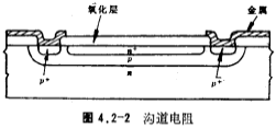
The P-well resistance in the CMOS circuit is about 1000~5000 ohms/square. When the P-well is diffused with drain-source phosphorus, the P-well channel resistance is shown in Figure 4.2-2, and its sheet resistance is higher. MOS tube resistance. However, the diffusion depth of the P-well and the lateral diffusion caused by it are about 5-10 microns, making it impossible to make the resistance bar narrow. In addition, a channel stop ring is needed between the P-well resistor bars to eliminate the leakage current of the surface inversion layer between the resistors, so its area is also considerable.
3. Ion implantation resistance
Using ion implantation instead of diffusion method to manufacture resistors, the amount of implanted ions can be flexibly controlled in a larger range. For example, when the implantation dose of boron is 1014/cm2, the sheet resistance is about a few hundred ohms per square, and when the implantation dose is At 1013/cm2, the sheet resistance is about several thousand ohms per square, and when the implant dose is 1012/cm2, the sheet resistance can reach tens of thousands of ohms per square. Therefore, if ion implantation is used to make a large resistor, the area occupied will not be too large. MOS tube resistance. In addition, since the implantation dose is easier to accurately control than the diffusion impurity amount, the accuracy of the ion implantation resistance is also higher than that of the diffusion resistance. However, when there are different reverse bias voltages between the pn junction formed between the ion implantation and the substrate; the width of the depletion layer is different, so that the carrier flow in the conductive layer changes, so the linearity of the resistance is not Ideally, the voltage coefficient of the resistor is relatively large, and at the same time, due to the influence of the surface charge of the oxide layer, the carrier concentration on the surface of the conductive layer is also unstable, so the accuracy of the large resistor is limited to a certain extent.
4. Polysilicon resistance
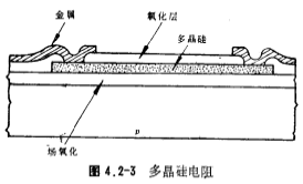
In the manufacturing process of MOS field effect transistors, polysilicon is used as electrode material (gate), and the structure of resistors made of polysilicon is shown in Figure 4.2-3. Its sheet resistance value is generally 30~200 ohm/square. When polysilicon is used as a high-resistance resistor, another photolithography can be added, and a smaller dose of ion implantation can be used to obtain the resistance. The resistance can reach 10 kilohms/square. MOS tube resistance. Because there is a thick oxide layer under the polysilicon to isolate the circuit, its parasitic capacitance is greatly reduced, but the sheet resistance of the polysilicon resistor is related to the ion implantation dose, the thickness of the polysilicon, the quality of the polysilicon deposition and other factors. Therefore, it is difficult to make precision resistors.
5. Thin film resistors
By sputtering, Ni-Cr or Cr-Si and other materials are deposited on the insulating layer of the silicon wafer in a certain proportion to obtain the thin film resistance. The sheet resistance value of the thin film resistor can be adjusted by the nature of the material used, the proportion of the composition and the thickness of the deposited layer. In general, the thin film

The thickness is several hundred to several thousand angstroms, the sheet resistance of Ni-Cr field oxidation is several hundred ohms/square, and Cr-Si is several hundred to several thousand ohms/square. The linearity of thin film resistors is the best, that is, the voltage coefficient is low. The temperature coefficient is also the lowest, about one part per million/℃, and has nothing to do with other manufacturing process conditions of the MOS circuit. MOS tube resistance. When the resistance accuracy is very high, it can also be adjusted by laser correction. Therefore, thin film resistors are a better way to manufacture precision matching resistors.
Contact: Mr. Zou
Contact number: 0755-83888366-8022
Mobile phone: 18123972950
QQ: 2880195519
Contact Address: 5C1, Block CD, Tianji Building, Tianan Digital City, Chegongmiao, Futian District, Shenzhen
Please search WeChat official account: "KIA Semiconductor" or scan the following picture to "Follow" official WeChat official account
Please "follow" the official WeChat account: provide MOS tube technical assistance


