The main parameters of MOS tube, 1. Drain-source cut-off current Ioff For enhanced MOS tube, when VGS=0, the tube is cut off and the drain-source cannot be conducted, that is, the drain-source current
The main parameters of MOS tube, 1. Drain-source cut-off current Ioff For enhanced MOS tube, when VGS=0, the tube is cut off and the drain-source cannot be conducted, that is, the drain-source current
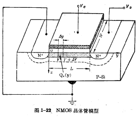
For the current-voltage characteristics of the unsaturated region, the MOS tube is a voltage control device. Under the action of the gate voltage, as long as the channel is formed, the MOS tube will w
For the current-voltage characteristics of the unsaturated region, the MOS tube is a voltage control device. Under the action of the gate voltage, as long as the channel is formed, the MOS tube will w
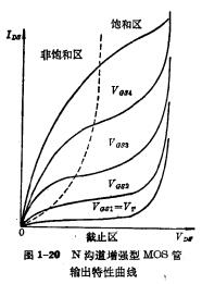
The output characteristic curve of the MOS tube can be displayed by the JT-1 graphic instrument like a bipolar tube, as shown in Figure 1-20. The working situation of the MOS tube has been briefly int
The output characteristic curve of the MOS tube can be displayed by the JT-1 graphic instrument like a bipolar tube, as shown in Figure 1-20. The working situation of the MOS tube has been briefly int
Threshold voltage of MOS device, MOS threshold voltage, threshold voltage VT The so-called threshold voltage of MOS device refers to the gate voltage when the drain source of the device is just turned
Threshold voltage of MOS device, MOS threshold voltage, threshold voltage VT The so-called threshold voltage of MOS device refers to the gate voltage when the drain source of the device is just turned
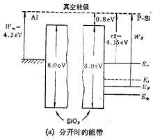
The MOS system on the silicon surface of the MOS system is more complicated. Therefore, in the absence of an external electric field, a space charge region may have been formed on the Si surface, and
The MOS system on the silicon surface of the MOS system is more complicated. Therefore, in the absence of an external electric field, a space charge region may have been formed on the Si surface, and

MOS capacitor-semiconductor physical device characteristics and MOS transistor capacitor MOS capacitor is a MOS system composed of metal-oxide-semiconductor, which can be regarded as a parallel plate
MOS capacitor-semiconductor physical device characteristics and MOS transistor capacitor MOS capacitor is a MOS system composed of metal-oxide-semiconductor, which can be regarded as a parallel plate
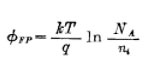
The surface potential of MOS structure, the physical basis of MOS transistors 1. The silicon surface of an ideal MOS system under the action of an external field 2. The surface potential and the charg
The surface potential of MOS structure, the physical basis of MOS transistors 1. The silicon surface of an ideal MOS system under the action of an external field 2. The surface potential and the charg
The physical basis of MOS transistors The structure, types and working principles of MOS transistors are briefly introduced above. In order to deeply understand the characteristics of MOS transistors,
The physical basis of MOS transistors The structure, types and working principles of MOS transistors are briefly introduced above. In order to deeply understand the characteristics of MOS transistors,
The characteristics of MOS field effect transistors: (1) low power consumption (2) small device geometry (3) simple manufacturing process, the characteristics of MOS field effect transistor is a surfa
The characteristics of MOS field effect transistors: (1) low power consumption (2) small device geometry (3) simple manufacturing process, the characteristics of MOS field effect transistor is a surfa
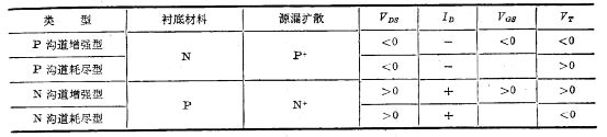
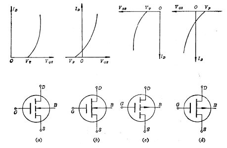
The types of MOS transistors can be divided into N-channel MOS transistors and P-channel MOS transistors according to the different conductive carriers. The type of MOS transistor of each channel can
The types of MOS transistors can be divided into N-channel MOS transistors and P-channel MOS transistors according to the different conductive carriers. The type of MOS transistor of each channel can


5C1, CD Block, Tianji Building, Tianan Digital City, Futian District, Shenzhen

KIA-The Public