Electronic Technology Forum
Basic Conceptual Characteristics and Characteristics of MOS Field Effect Transistor
(1)Low power consumption
The characteristic of MOS field effect transistor is a surface device, and its working principle, conduction mechanism and manufacturing method are very different from bipolar transistors.
MOS transistorIt is a voltage control device, and a bipolar transistor is a current control device. Turning on a bipolar transistor needs to provide current to the base; turning on a MOS transistor only needs to provide a voltage on the control gate. Since the gate source is separated by an oxide film insulating layer with an impedance of more than 101Ω, it has a very high input impedance. For enhancement mode MOS transistors, there are two "back-to-back" PN junctions between the drain and source, so there is no direct path between the gate source and the drain source. Therefore, the power consumption of the MOS transistor is very low, and it can maintain operation almost without consuming input power, which is more important for MOS integrated circuits.

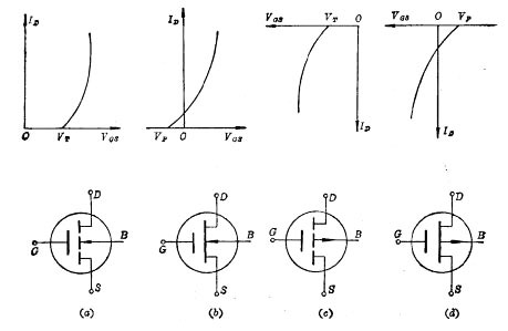
NMOS enhancement mode NMOS depletion mode PMOS end strong mode PMOS depletion mode
Figure 1-8 The transfer characteristics and symbols of the four types of MOS transistors
(2)Small device geometry
Due to the simple structure of the MOS transistor, the geometric size of the MOS transistor can be made small. Especially in integrated circuits, dozens of MOS transistors can be placed in the area equivalent to a bipolar transistor, so the integration of MOS circuits can be greatly improved.
(3)Simple manufacturing process
The manufacturing process of MOS transistors is simpler than that of bipolar transistors, as long as one diffusion, two oxidations, four photolithography, and fewer high-temperature passes. Therefore, it is easy to control and the yield is high.
The characteristics of MOS field effect transistors, but MOS transistors also have its shortcomings, mainly due to the slower switching speed and lower operating frequency. The operating speed of MOS integrated circuits is 10 to 100 times slower than equivalent bipolar integrated circuits, or even more. However, in recent years, through various improvements, the switching speed of MOS transistors has been greatly improved.
Contact: Mr. Zou
contact number:0755-83888366-8022
mobile phone:18123972950
QQ:2880195519
Contact Address: 5C1, Block CD, Tianji Building, Tianan Digital City, Chegongmiao, Futian District, Shenzhen
Please search WeChat official account: "KIA Semiconductor" or scan the following picture to "Follow" official WeChat official account
Please "follow" the official WeChat account: provide MOS tube technical assistance


