Electronic Technology Forum
Analysis of the surface potential of the MOS tube structure and the charge in the space charge region
From the above discussion, the size of the surface potential φs is a quantity that characterizes the amount of charge in the space charge region. Their quantitative relationship is very useful in the following discussion.


1. MOS surface potential
The surface potential of the space charge region of the semiconductor surface at the Si-SiO2 interface can be obtained by solving the Poisson equation. In general, there are ionized acceptors N2 and donor NA, as well as electrons and holes P in the space charge region. Therefore, the charge density of the space charge region can be written as:

However, under the approximate conditions of the depletion layer, the charge density of the space charge region can be simplified to Q(χ)=-qNA. Because the P-type semiconductor is considered, ND in the space charge region ≈ 0; when depleted, the hole concentration in the space charge region p(χ) << NA; and when φs<2φF, the electrons in the space charge region Concentration n (χ) "NA. Therefore, Q(χ)=-9NA under the depletion approximation. Substituting it into the Poisson equation, we get:

This equation is consistent with the Poisson equation when analyzing the depletion layer of the PN junction. Solve this equation as follows:
First, rewrite the formula (1-5) as:

Use the method of separating variables to integrate on both sides:

That is, the electric field intensity at χ where the electric field is located between the space charge zone and the Si-Si02 interface is obtained, where χ4 is the width of the depletion layer (space charge. Charge zone).

Then put  , and use the method of separating variables to integrate on both sides :

That is to say, the electric potential at the space charge area χ from the Si-SiO2 interface is:

When χ=0, (0)≈φs. which is:

The width of the depletion layer is the width of the space charge region here, which can be written as:

This result is similar to the width of the space charge region of the unilateral abrupt junction PN junction. If the strong inversion condition φs=2φF is satisfied, then the maximum width of the space charge region is:

2. The charge density of the space charge region
According to equation (1-9), we can get the amount of charge per unit area in the space charge region as:

If NA-1018/cm3 and φs are 0.2V and 0.4V respectively, the space charge density per unit area can be obtained: 2.5×10⁻⁸C/cm2 and 3.6×10⁻⁸C/cm2.
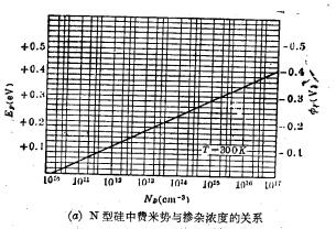
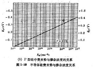
It can be seen from formula 1-8 that the higher the doping concentration, the greater the surface potential to achieve strong inversion, which is consistent with the strong inversion condition φs=2φF mentioned earlier. MOS structure surface potential
Contact: Mr. Zou
Contact number:0755-83888366-8022
Mobile phone:18123972950
QQ:2880195519
Contact Address: 5C1, Block CD, Tianji Building, Tianan Digital City, Chegongmiao, Futian District, Shenzhen
Please search WeChat official account: "KIA Semiconductor" or scan the following picture to "Follow" official WeChat official account
Please "follow" the official WeChat account: provide MOS tube technical assistance


