Electronic Technology Forum
MOS tube current-voltage characteristic equation-saturated region and non-saturated region
The MOS tube is a voltage control device. Under the action of the gate voltage, as long as the channel is formed, the MOS tube will work in the saturated or unsaturated zone (the device breakdown is not considered). The saturated region and the unsaturated region are divided by whether the channel at the drain is pinched off, and the characteristic curve is divided by VDS greater than (VGS-VT) or less than (VGS-VT). MOS tube current and voltage characteristics. Let's study the quantitative relationship between the channel current and the gate voltage and drain voltage in the unsaturated and saturated regions respectively.
1、Current-voltage characteristics in the unsaturated zone
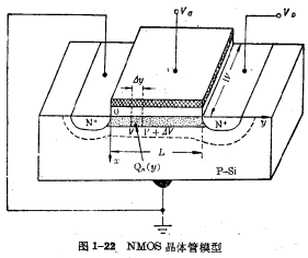
Figure 1-22 shows the structure model of the N-channel MOS tube, where the source is grounded. In order to establish the mathematical relationship, suppose that the source and the substrate are defined as the coordinate origin o at the intersection point of the surface, The direction is specified as pointing from the origin to the Si substrate,
 The direction is defined as pointing from the origin to the drain diffusion area. Under the action of VG, the inversion layer forming the conduction is very thin, such as about 10nm.Between source and drain (along
  direction) Under the action of the electric field, it becomes a current channel. It can be seen that the current of the MOS tube is composed of a thin layer of current parallel to the Si surface. Suppose the channel length is L, the width is W, and VD≈0, that is, the device is fully working in the unsaturated region, and the inversion channel is fully formed from the source to the drain without pinch-off points. MOS tube current and voltage characteristics.

Next, we will analyze and derive the current-voltage characteristic equation of the unsaturated zone.
Let us first consider a small section of the channel area  . Hypothesis
 The channel voltage drop at is:

 Is the channel current along the direction of
  , dR is the channel
  The channel resistance of the section, here

Among them, A is the channel cross section at 
 ,then:

Among them,  is the channel resistivity,
  is the surface electron mobility,
 Is the electron density of the channel
  .
.
so

In The amount of charge per unit area in the point channel is:

Substituting (1-32) into the formula:

After finishing:

As we all know, when the gate voltage is equal to the threshold voltage, the channel has just been formed. If the gate voltage further increases and exceeds the threshold voltage , an increase in charge will be generated per unit area of the metal gate
 The charge per unit area generated on the other side of the oxide layer capacitor
  is Movable charge per unit area in the channel
 Obviously,
 Will land in the trench, the value of
  is:
is:

Among, Is the voltage drop of the drain-source voltage at
  .So the charge density in the
  point channel is:

Substituting formula (1-37) into formula (1-35), we get:

Integrate both sides of (1-88) to obtain the current-voltage characteristic equation of the unsaturated region of the MOS tube.

Therefore, the channel current equation in the unsaturated zone is:

2、Current-voltage characteristics in the saturation region
The above analysis assumes that a good channel is formed everywhere on the Si surface under the gate, and the VD is very small. But when VD increases to a certain value, due to the effect of VD, the channel near the drain under the gate is pinched off. In this case, it is said that the channel current has reached "saturation". Obviously, the movable channel charge at the pinch-off point is equal to zero, namely:

so:

This is the condition for the MOS tube to enter the saturation zone. Substituting this condition into the equation (1-39), the channel current-voltage characteristic equation of the saturation zone is obtained.

3、The leakage-source current formula and conduction factor of MOS tube
(1)Current formula
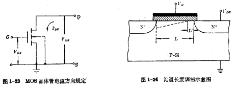
The following rewrite formulas (1-39) and (1-41) into a form suitable for common use in engineering design. We stipulate the reference point of the source voltage. The current flowing from the drain to the source is the positive current direction, which is expressed by IDS. The current and voltage characteristics of the MOS tube are shown in Figure 1-23.
When VDS<VGS-VT, the MOS tube works in the unsaturated zone, according to  , the N-channel MOS tube drain-source current formula can be written as:

When  , the leakage of the saturation region can be written The source current formula is:

If so

So the current formula of the MOS tube can be rewritten as:

These two formulas are also applicable to PMOS transistors. The difference is that the direction of drain-source current is opposite to that of NMOS transistors, so add a negative sign before the formula.
It is more convenient to use these two current formulas to explain the characteristic curve. When VDS is constant, IDS increases with the increase of VGS, indicating that with the increase of VGS, the channel widens. In the unsaturated zone, the VDS is very small, the  item in the formula is OK Omit,So IDS increases linearly with VGS: but when VGS is large (still in the unsaturated zone),
  cannot be omitted, so

IDS gradually slows down with the increase of VGS, and the characteristic curve gradually curves, that is, the channel resistance gradually increases.
In the saturation region, the leakage current formula has nothing to do with VDS, so IDS does not rise with the increase of VGS. However, actual measurement shows that IDS also increases with the increase of VGS. This is because the actual channel is modulated by the drain voltage, so that the actual channel length decreases as the VGS increases, as shown in Figure 1-24. Where L is the channel length, and L'is the distance from the pinch point of the channel to the edge of the drain diffusion region, which can be approximated by the learning edge abrupt junction:

Therefore, as the VDS increases, L'increases, and the effective channel length L-L' decreases accordingly, so IDS increases slightly with the increase of VGS. To make the output characteristic curve of the saturation region relatively flat, the channel length can be made longer in the design.
(2)Conductivity factor
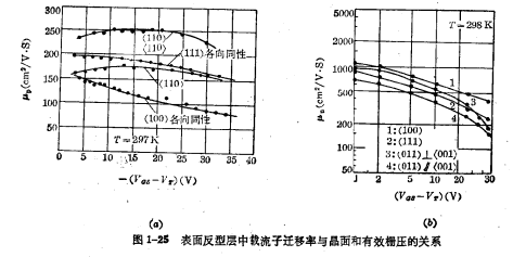
In the current formula, k is usually called conductivity factor or k constant, and k'is called intrinsic conductivity factor or intrinsic k constant, and its unit is A/V2 or mA/V2, in the design of MOS tube, k'constant It is an important parameter. It can be seen from the formula (1-44) that the intrinsic conductivity factor k'is not only directly related to the process, but also directly related to the average carrier mobility in the inversion layer. related. Experiments have proved that the average mobility of carriers in the inversion layer is lower than that in the body, and is related to the crystal orientation of the substrate material, impurity concentration, gate voltage, and process conditions. Figure 1-25 shows the relationship between the carrier mobility in the inversion layer and the crystal orientation and effective gate voltage. Figure 1-25(a) shows the experimental results of hole mobility, and Figure 1-25(b) shows the experimental results of electron mobility. In the production of P-channel MOS circuits, the substrate material often chooses (100) or (111) Si single wafer. Hole mobility can generally be taken from the figure during design calculation:


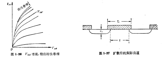
The electron mobility in the N-type inversion layer is generally considered to be about 3 times higher than the hole mobility on the surface. In the design, often take  This value is about the migration rate in the body half. The surface mobility is lower than the in vivo mobility. There are roughly two reasons: the main reason is that there are many defects on the surface to form scattering centers, which makes the surface scattering stronger than in the body; in addition, in the channel region, there is movement with carriers. The strong electric field in the vertical direction increases the carrier concentration in the inversion layer and increases the scattering probability of the Si-SiO2 interface, so the surface mobility decreases. In the actual measurement, when VGS is high, the output characteristic curve will shrink with the increase of VGS. The current and voltage characteristics of the MOS tube are shown in Figure 1-26. It must also be pointed out that in the specific calculation of the k factor, the actual channel length should be taken as the value after deducting the lateral diffusion, namely
 For the junction depth, L is the size of the photolithography mask design, as shown in Figure 1-27.


Contact: Mr. Zou
Contact number:0755-83888366-8022
Mobile phone:18123972950
QQ:2880195519
Contact Address: 5C1, Block CD, Tianji Building, Tianan Digital City, Chegongmiao, Futian District, Shenzhen
Please search WeChat official account: "KIA Semiconductor" or scan the following picture to "Follow" official WeChat official account
Please "follow" the official WeChat account: provide MOS tube technical assistance


