Electronic Technology Forum
Qualitative Discussion and Analysis of MOS Tube Output Characteristic Curve
The working situation of the MOS tube has been briefly introduced above, and now we will further analyze the output characteristics of the MOS tube. The so-called output characteristic of MOS tube refers to the law of the change of drain-source current IDS with drain-source voltage when the gate-source voltage is constant.
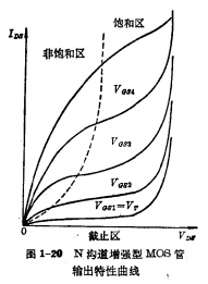
The bias voltage and transfer characteristics of the entire MOS tube (take N-channel as an example) during operation are shown in Figure 1-2. The output characteristic curve of the MOS tube can be displayed by the JT-1 graphic instrument like a bipolar tube, as shown in Figure 1-20.

Each curve in the figure corresponds to a gate voltage VGS, and the bottom curve corresponds to VGS-VT. It can be seen directly from the figure that when VGS≤VT, IDS is almost zero and does not change with VGS. At this time, the channel has not yet been formed or has just been formed.
When VGS exceeds VT for a certain value, the channel has been formed, and IDS will vary with VDS. When VDS is small, IDS increases as VGS increases. After VDS increases to a certain value (the dotted line is the boundary in the figure), the increase of VDS does not obviously cause the increase of IDS, and we think that the current is saturated at this time. If VGS is further increased to a certain value, IDS rises sharply, and the PN junction of the drain region is reversed breakdown at this time. In summary, the output characteristic curve of the MOS tube can be divided into four regions. The left side of the dashed line in the figure is the unsaturated zone, and the right is the saturated zone. The area where the current surges is called the breakdown zone, and the area IDS=0 under VGS≤VT is called the cut-off zone. The output characteristics of the MOS tube, and why the output characteristic curve of the MOS tube has the unsaturated zone and the saturated zone, this is a problem that we need to study.
1. Unsaturated zone
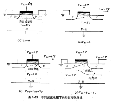
When VG>VT and VDS=0, a channel will be formed, and the thickness of the channel is the same from source to drain, as shown in Figure 1-21(a). If VGS>VT, and a small bias voltage VDS is applied from the source to the drain, the width of the channel from the drain to the source will not be the same. Because the voltage at the source end of the channel region is zero, and the voltage at the drain end is VDS, the potential of each point of the channel along the source-drain direction is different. Therefore, the potential difference between the gate and the channel at the source end through SiO2 is VGS, and the channel voltage between the gate and the drain end is (VGS-VDS), and the middle is the excess voltage zone. This shows that the voltage drop at each point in the channel region under the gate is different, and the electric field is of course also different. In this way, the thickness of the channel will gradually decrease along the drain direction, and the distribution of the carrier concentration in the inversion layer will also gradually decrease along the drain direction, as shown in Figure 1-21(b). In this case, the entire channel region can be regarded as a resistance, so the current IDS increases with the increase of VGS. However, because the increase of VDS will make the channel thinner along the drain direction, that is, the channel resistance will increase correspondingly with the increase of VDS, so the increase of IDS does not increase linearly with VDS, but gradually slows down its increase. s speed. As shown in the right part of the unsaturated zone in Figure 1-20.
2. Saturation zone
When VDS=VGS-VT, the channel at the drain is pinched off (the depletion region still exists), as shown in Figure 1-21(c). If VDS continues to increase to VDS>VGS-VT, it enters the saturation zone. At this time, the effect of the drain-source voltage will further increase the pinch-off area of the channel. This area becomes the area with the greatest resistance in the current path between the source and the drain, so the voltage between the drain and the source will inevitably fall here, so that the pinch The broken area has a large electric field. The output characteristics of the MOS tube. In addition, there is a non-pinch-off N-type channel on the left side of the pinch-off region. The situation here is similar to that in the unsaturated state. The electrons emitted from the source can migrate through the channel. After the pinch-off area, it will be swept into the drain area under the action of the strong electric field in the pinch-off area. After the channel is pinched off, the drain voltage that is further increased basically falls in the pinch off region, and the electric field distribution in the channel that is not pinched off basically does not increase with VDS, and of course IDS does not increase with VDS.

If the VGS increases, the initial thickness of the channel increases, and the drain-source voltage of the characteristic curve entering the saturation region also increases, but the relationship of VDS=VGS-VT is always satisfied.
Contact: Mr. Zou
Contact number:0755-83888366-8022
Mobile phone:18123972950
QQ:2880195519
Contact Address: 5C1, Block CD, Tianji Building, Tianan Digital City, Chegongmiao, Futian District, Shenzhen
Please search WeChat official account: "KIA Semiconductor" or scan the following picture to "Follow" official WeChat official account
Please "follow" the official WeChat account: provide MOS tube technical assistance


