Electronic Technology Forum
Simple realization of SiO2 on silicon surface of MOS system
As mentioned earlier, the actual MOS system on the silicon surface of the MOS system is more complicated. Therefore, in the absence of an external electric field, a space charge region may have been formed on the Si surface, and the energy band may be bent. The silicon surface of the MOS system. The following will discuss the different work functions of metals and semiconductors and the effect of the effective surface state charge density in the gate oxide on the Si surface.
1. The influence of work function difference
The work functions of metals and semiconductors are different, and silicon dioxide is not completely insulated. Therefore, electrons will be exchanged between the metal and semiconductor through the oxide layer to form a space charge zone on the Si surface, and band bending occurs.
The so-called work function refers to the minimum energy required for an electron with an initial energy equal to the Fermi energy EF to escape from the inside of a metal or semiconductor into a vacuum.
Suppose the work function of metal (take AI as an example) is ,The work function of a semiconductor (take Si as an example) is
 ,As shown in Figure 1-12 (a). The silicon surface of the MOS system. If the two systems are combined, because the work function of the metal AI is smaller than the work function of the semiconductor, some electrons are transferred from the metal to the semiconductor surface. The metal surface is positively charged due to lack of electrons, and the semiconductor surface is negative due to excess electrons. In the space charge region of the electric charge, the energy band of the Si surface is bent downward. When equilibrium is reached, the contact potential difference between the metal AI and the semiconductor is
 . Here, the metal side is high potential, and the semiconductor side is the silicon surface of the low potential MOS system. As shown in Figure 1-12(b).
 The relationship with work function is:

If the energy band is to be flattened, a voltage must be applied to the metal gate to offset the influence of the work function difference on the energy band. As shown in Figure 1-12 (c). This voltage is:

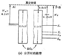
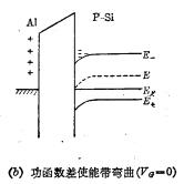
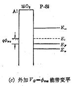
Figure 1-12 The influence of the metal semiconductor common function on the energy band
The following is a brief description of which factors are related to the contact potential difference.
Work function difference  The size is not only related to the selected The metal material is related to the silicon type and doping concentration. Figure 1-13 shows the difference in work function between aluminum and gold electrodes on oxidized N-type and P-type silicon
 Relationship with silicon impurity concentration. It can be seen from the figure that the work function difference between metal A1 and semiconductor Si is generally less than zero, while the work function difference between gold and semiconductor is generally greater than zero.
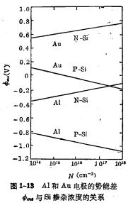
If the doping concentration is  N-type Si, The work function difference with A1 can be found from Figure 1-15 to be -0.3V. For P-type Si with the same doping concentration, the work function difference with A1 is about -0.9V.
2. The effect of effective surface state charge in the oxide layer
The so-called effective surface state charge is a concept introduced to deal with problems. It regards fixed positive charges (mainly oxygen vacancies), movable positive charges (mainly sodium ions), and the interface states existing on the interface of Si-SiO as being concentrated in SiO. The silicon surface of the MOS system. The positive charge near the Si-SiO2 interface, its surface charge density is used Express.
 The size of, particularly obviously depends on the process level and process conditions. Because it acts as a positive electric center, it is equivalent to applying a positive electric field to the Si surface, which induces a negatively charged space charge area on the Si surface, causing the energy band to bend downward, as shown in Figure 1-14.
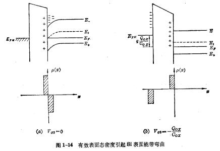
To flatten the energy band, a gate voltage must be applied to the metal gate , To offset the effective surface state charge density
 The influence on the energy band makes the Si surface no longer have a space charge zone, and the metal surface induces
 Equal amount of negative charge
 < span style="font-size: 18px;">. According to the definition of capacitance, the oxide layer capacitance can be written as:

Therefore, the external voltage applied to the metal electrode to flatten the energy band is:

Contact: Mr. Zou
Contact number:0755-83888366-8022
Mobile phone:18123972950
QQ:2880195519
Contact Address: 5C1, Block CD, Tianji Building, Tianan Digital City, Chegongmiao, Futian District, Shenzhen
Please search WeChat official account: "KIA Semiconductor" or scan the following picture to "Follow" official WeChat official account
Please "follow" the official WeChat account: provide MOS tube technical assistance


