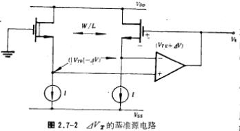
MOS tube voltage bias circuit, which is often used in MOS analog integrated circuits, has become an important part of the circuit. However, these bias circuits have common shortcomings. The current it
MOS tube voltage bias circuit, which is often used in MOS analog integrated circuits, has become an important part of the circuit. However, these bias circuits have common shortcomings. The current it
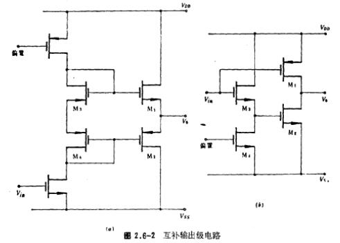
CMOS complementary output stage, CMOS devices can be used to form a complementary output stage similar to the bipolar circuit, as shown in Figure 2.6-20. In the figure, M1 and M2 constitute the comple
CMOS complementary output stage, CMOS devices can be used to form a complementary output stage similar to the bipolar circuit, as shown in Figure 2.6-20. In the figure, M1 and M2 constitute the comple

MOS output stage circuit, when designing the output stage of an operational amplifier, it is necessary to consider its ability to drive a load (in MOS circuits, the load is mainly a capacitor), output
MOS output stage circuit, when designing the output stage of an operational amplifier, it is necessary to consider its ability to drive a load (in MOS circuits, the load is mainly a capacitor), output
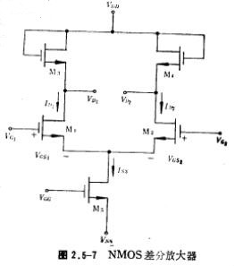
For NMOS differential amplifiers, to increase the gain of NMOS differential amplifiers, depletion-type devices can be used for M3 and M4, but the voltage gain of NMOS differential amplifiers is much l
For NMOS differential amplifiers, to increase the gain of NMOS differential amplifiers, depletion-type devices can be used for M3 and M4, but the voltage gain of NMOS differential amplifiers is much l
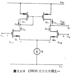
CMOS differential amplifier, the working current of the differential amplifier is provided by the current source IO. Obviously, the working principle of this circuit is the same as the circuit in Figu
CMOS differential amplifier, the working current of the differential amplifier is provided by the current source IO. Obviously, the working principle of this circuit is the same as the circuit in Figu
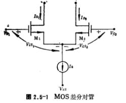
The main characteristics of MOS differential pairs are shown in Figure 2.5-1. M1 and M2 in the figure are completely symmetrical (matched), and their working currents (ID1, ID2) are provided by the cu
The main characteristics of MOS differential pairs are shown in Figure 2.5-1. M1 and M2 in the figure are completely symmetrical (matched), and their working currents (ID1, ID2) are provided by the cu
CMOS single-stage amplifier Fig. 2.4-1c, dCMOS single-stage amplifier Compared with Fig. 2.4-1a, bNMOS single-stage amplifier, it has higher voltage gain and lower power consumption. The gain is gener
CMOS single-stage amplifier Fig. 2.4-1c, dCMOS single-stage amplifier Compared with Fig. 2.4-1a, bNMOS single-stage amplifier, it has higher voltage gain and lower power consumption. The gain is gener
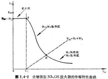
NMOS single-stage amplifier, 1. Fully enhanced NMOS amplifier (Figure 2.4-1a) (1) The input-output transmission characteristic curve of the amplifier. The amplifier has three working states: i, the in
NMOS single-stage amplifier, 1. Fully enhanced NMOS amplifier (Figure 2.4-1a) (1) The input-output transmission characteristic curve of the amplifier. The amplifier has three working states: i, the in
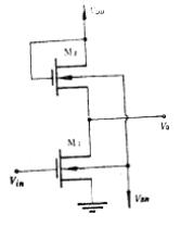
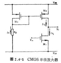
MOS single-stage amplifier. In MOS (NMOS and CMOS) operational amplifiers or other analog circuits, the common source MOS amplifier with active load is the most commonly used. There are four commonly
MOS single-stage amplifier. In MOS (NMOS and CMOS) operational amplifiers or other analog circuits, the common source MOS amplifier with active load is the most commonly used. There are four commonly
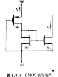
The bias circuit of the CMOS tube, the so-called CMOS bias circuit, is to replace the bias resistor image.png in Figure 2.3-1 with a P-channel MOS tube. The circuit form is shown in Figure 2.3-5, in 1
The bias circuit of the CMOS tube, the so-called CMOS bias circuit, is to replace the bias resistor image.png in Figure 2.3-1 with a P-channel MOS tube. The circuit form is shown in Figure 2.3-5, in 1


5C1, CD Block, Tianji Building, Tianan Digital City, Futian District, Shenzhen

KIA-The Public