Electronic Technology Forum
Analysis and interpretation process of bias circuit of NMOS tube
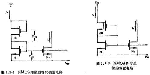
There are two types of bias circuits for NMOS transistors. One is the bias circuit with an enhanced transistor as the equivalent resistance, and the other is the bias circuit with a depletion transistor as the equivalent resistance. The circuit forms are shown in Figure 2.3. -2, as shown in Figure 2.3-3.

The M2 tube in Figure 2.3-2 and Figure 2.3-3 is equivalent to the bias resistor RB in Figure 2.3-1. It can be seen from the current-voltage characteristics of the MOS tube to reduce the channel width-to-length ratio of the MOS tube (W/ L), that is, increasing the channel length L can increase the equivalent resistance value at both ends of the drain source (the equivalent resistance here refers to the DC equivalent resistance, (VDS/ID)). If the channel width to length ratio of the M1 and M2 tubes is determined, the reference current IR is also determined. Conversely, given the reference current IR and the working voltage (VGS) of the M1 and M₂ tubes, the channel width-to-length ratio of the M1 tube and the M2 tube can be calculated respectively. Let's discuss the circuit in Figure 2.3-2 first.
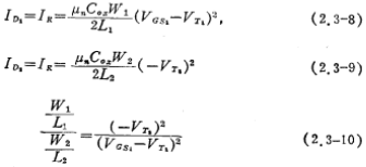
It can be seen from Figure 2.3-2 that the drain-source current ID of the M1 tube and the M2 tube is the same, which is equal to IR. According to the current equation, we can get

Obtained by the above two equations

The above-mentioned threshold voltage VT1, VT2. Respectively expressed as (see Chapter 1 (1.2-19) formula)

According to (2.3-5) and (2.3-7), the channel width to length ratio of the M1 and M2 tubes can be obtained. Now give an example
IR=80μA, VDD=2.5V, VSS=-2.5V, VT=1V, μn=600cm2/Vsec, tox=1000A, Io=200μA.
For simplicity, suppose the substrate of the M2 tube is connected to the source, try to calculate the channel width-to-length ratio of M1, M2, and M3.
From (2.3-5) formula

The VGS of the M2 tube is

From (2.3-7) formula

The relationship between the current source IO and IR in the figure is

The channel width to length ratio of the M3 tube is

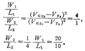
If L1=L2=L3=10 microns,
W1=80 microns, W2=20 microns, W3=200 microns.
From the formula (2.3-5~7) and the above example, it can be seen that under the conditions of a given IR, the larger the VGS of the MOS tube, the smaller the channel width-to-length ratio. In order to increase the voltage dynamic range of the current source IO output, usually the voltage value is relatively low. Therefore, when the power supply voltage (VDD, VSS) is large, it is bound to increase the M2 tube
 , Greatly reducing the width to length ratio of the channel. If the power supply voltage in the above example is changed to VDD=7.5V and Vss=-7.5V, then
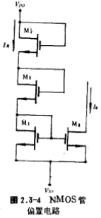
 volts, W2/L2=W2/269L1, that is, the channel width to length ratio of the M2 tube is reduced from W1/4L1 to W1/269L1. In order not to reduce the channel width to length ratio of the M2 tube too much, Figure 2.3-4 can be used
The circuit form.

For the bias circuit in Figure 2.3-3, the following expression can also be obtained.

where it is the pinch-off voltage of the depletion-type MOS tube M2, and its value is negative. The design method of the NMOS tube circuit in Figure 2.3-3 and Figure 2.3-4 is the same as that of the circuit in Figure 2.3-2.
Contact: Mr. Zou
Contact number: 0755-83888366-8022
Mobile phone: 18123972950
QQ: 2880195519
Contact Address: 5C1, Block CD, Tianji Building, Tianan Digital City, Chegongmiao, Futian District, Shenzhen
Please search WeChat official account: "KIA Semiconductor" or scan the following picture to "Follow" official WeChat official account
Please "follow" the official WeChat account: provide MOS tube technical assistance


