Electronic Technology Forum
Analysis of active resistance of MOS field effect transistor connection method
1. Source AC grounding
Figure 2.1-6a and b respectively represent the active resistance of the source of the N-channel and P-channel enhanced MOS transistors to AC ground.
(1) Saturated area (VDS≥VG-VT)
active resistor ro is
 < /span>
(2) Linear area (VDS<VG-VT) active ro The resistance is

2, drain AC grounding
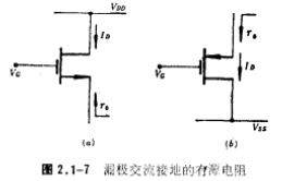
Figure 2.1-7a and b respectively show the active resistance of the drain of the N-channel and P-channel enhancement mode MOS transistors to AC grounding.
 < /span>
According to the small signal AC equivalent circuit, it is easy to find rois

When working in the saturation zone, , the above formula can be written as
 < /span>
When working in the unsaturated zone, (2.1-10) the  represented as
 < /span>
 < /span>
The above analysis shows that the output impedance is higher when the source is AC grounded. Therefore, in MOS amplifiers, in order to increase the voltage gain, the source AC ground is usually used as the amplifier's Active load.
Contact: Mr. Zou
Contact number: 0755-83888366-8022
Mobile phone: 18123972950
QQ: 2880195519
Contact Address: 5C1, Block CD, Tianji Building, Tianan Digital City, Chegongmiao, Futian District, Shenzhen
Please search WeChat official account: "KIA Semiconductor" or scan the following picture to "Follow" official WeChat official account
Please "follow" the official WeChat account: provide MOS tube technical assistance


