Electronic Technology Forum
Analysis of active resistance of MOS FET gate-drain connection
The main applications of MOS FETs in MOS analog integrated circuits are as follows: One is as an active load of the amplifier to improve the gain of the amplifier and the integration of the circuit The second is as a variable linear resistance to achieve gain control of the amplifier or control the feedback strength of the oscillator; MOS tube gate-drain active resistance. The third is to form a voltage divider circuit as an equivalent resistance. The active resistance of the MOS tube has the following forms.
1. Active resistance of MOS field effect transistor gate-drain connection
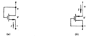
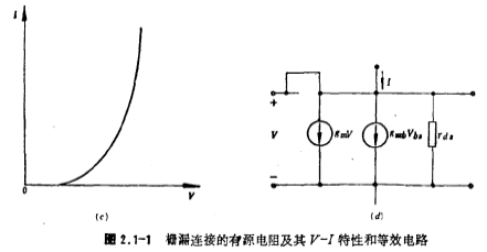
The active resistance (enhanced FET) connected to the gate and drain of the MOS FET is shown in Figure 2.1-1a, b. For n-channel devices, the source is usually connected to the negative end of the power supply voltage to eliminate the substrate effect. Similarly, the source of the P-channel device is connected to the positive terminal of the power supply voltage, which can also eliminate the substrate effect. MOS transistor gate-drain active resistance. Because VGS=VDS==V, so the picture The VI characteristics of 2.1-1a and b active resistors are shown in Figure 2.1-1c. Since the gate and drain are connected and work in the saturation region, its V-I characteristic can be expressed as:


令 , (2.1-1) formula can also be written as voltage form, namely (2.1-2)

If VDS=0, use (2.1-1) or (2.1-3) The formula can be obtained as shown in Figure 2.1-1a, the equivalent resistance of the bMOS FET, and its resistance value is

From the formula in Chapter 1 (1.3-37), the equivalent resistance of the above formula is ro Equal to the reciprocal of transconductance gm, ie

We can also use Figure 2.1-1d small signal equivalent circuit to calculatero, its expression is

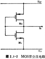
It can be seen from the above formula that to increase the resistance of the active resistor connected to the gate-drain of the MOS tube, the width W of the channel can be reduced, and the length L of the channel can be increased, that is, the width-to-length ratio of the channel can be reduced. Due to the limitation of the geometric size, the RO cannot be made very large, so when the enhanced MOS tube connected with the gate and drain is used as the load of the amplifier, the voltage gain is small. However, this kind of active device can be used to form a voltage divider, the form of which is shown in Figure 2.1-2.

Now consider the design method of the figure. Suppose the parameters in the figure are; VDD=5V, Vss=-5V, VT=±1V, ,
,
 , the required output voltage VG = 1 volt,
 , according to the formula (2.1-1), we can get:


From the above formula, the width-to-length ratio of M1 and M2 tubes can be obtained as:

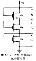
The voltage divider can also be composed of all NMOS tubes, and its form is shown in Figure 2.1-3. According to the size of the divided voltages V1, V2, V3, the value of the working current ID and considering the substrate bias effect of the M2 and M3 tubes, the aspect ratio of M1, M2 and M3 can be obtained using the formula (2.1-1).

relevant information
Active resistance of MOS gate-source connection
N-channel die type as active resistor
Active resistance of MOS field effect transistor connection mode
Contact: Mr. Zou
Contact number: 0755-83888366-8022
Mobile phone: 18123972950
QQ: 2880195519
Contact Address: Block 5C, CD Block, Tianji Building, Tianan Digital City, Chegongmiao, Futian District, Shenzhen
Please search WeChat official account: "KIA Semiconductor" or scan the following picture to "Follow" official WeChat official account
Please "follow" the official WeChat account: provide MOS tube technical assistance


