Electronic Technology Forum
Analysis Model of Short Channel Threshold Voltage of MOS Field Effect Transistor
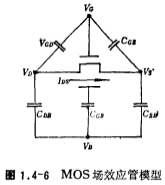
MOS FET model shown in Figure 1.4-6.

The main parameter relations and process parameters of MOS FET are as follows (see reference [12] for details);
1, threshold voltage VT

where a is the short channel correction coefficient, 
2, carrier mobility μ

where μ is in the formula. It is the low electric field carrier mobility.
θ is the correction factor for mobility.
3. Drain voltage when entering the saturation zone

4. Channel length modulation

where L is the design value of the channel length,  is the diffusion depth (junction depth), and the short-channel MOS threshold voltage model a is the lateral correction coefficient of the diffusion.
(1) Linear zone

(2) Saturation zone

where
5. The effective width of the channel width W

Where W is the design value of the channel width, and xw is the thickness of the field oxide layer
6. MOS field effect tube current IDS
(1) Linear zone

(2) Saturation zone
Use the formula (1.4-21) for VD in the formula (1.4-26) Instead, short-channel MOS threshold voltage model. The IDS relational expression of the saturation zone can be obtained.
(3) Cut-off area (VG-VS<VT)

7. MOS capacitors (CGS, CGD, CGB)
(1) Linear zone
(2) Saturation zone

(3) Cut-off area

8. Junction capacitance

where
W and L are the width and length of the drain or source diffusion area, respectively, Is the contact potential of the p-n junction.
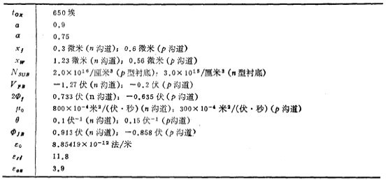
9. The main parameters of CMOS process

Contact: Mr. Zou
Contact number: 0755-83888366-8022
Mobile phone: 18123972950
QQ: 2880195519
Contact Address: Block 5C, CD Block, Tianji Building, Tianan Digital City, Chegongmiao, Futian District, Shenzhen
Please search WeChat official account: "KIA Semiconductor" or scan the following picture to "Follow" official WeChat official account
Please "follow" the official WeChat account: provide MOS tube technical assistance


