Electronic Technology Forum
Basic Forum Analysis of MOS Tube Bias Circuit
In MOS analog integrated circuits, the bias circuit is an indispensable and important part. The bias circuit is closely related to the constant current source circuit in the previous section. In the second section, we discussed the constant current characteristics and output impedance of the constant current source circuit, and how to realize the reference current IRThere is no explanation, this section will focus on the reference current source IRHow to achieve it. IRAfter the decision is made, the channel width to length ratio (W /L) Design the required constant current source current IO.
1. MOS tube bias circuit
The basic bias circuit is shown in Figure 2.3-1. The reference current IR is determined by the resistance RB, power supply voltage (VDD, Vss) and M 2The VGS of the tube is determined by the voltage, ie< /span>

M2The tube works in the saturation zone, and its current can be expressed by the following formula

From the above formula, we can get M1The tube aspect ratio is

The above-style , the voltage value is small,
 So the above formula can be simplified to< /span>

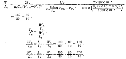
Using formulas (2.3-1) and (2.3-4), for a given I< span style="font-size: 10px;">R, power supply voltage (VDD, VSS) and M1 tube of VGS voltage, you can get  and M1 The width to length ratio of the tube W1/L1, an example is as follows:
[example] IR=80 microamperes, VDD=5 volts, V span>SS=-5 volts, VGS1=2 volts, VT=1 volt ,ΜD=600cm2/volt ●seconds,
toх=1000 angstroms, Io1=100 microamperes, Io2=200 microamperes, εo=8.85×10⁻¹⁴ method/cm, εoх=3.9.
Trial calculation .
.
By (2.3-1) formula

By (2.3-4) formula

Take L1=L2=L3=10 microns,
Then W1=80 microns, W2=100 microns, W3=200 microns.
The bias resistor RB in Fig. 2.3-1 has a large resistance value and needs to occupy a larger silicon chip area. In order to improve the integration, the RB resistor can be replaced by a MOS tube.
relevant information
Contact: Mr. Zou
Contact number: 0755-83888366-8022
Mobile phone: 18123972950
QQ: 2880195519
Contact Address: 5C1, Block CD, Tianji Building, Tianan Digital City, Chegongmiao, Futian District, Shenzhen
Please search WeChat official account: "KIA Semiconductor" or scan the following picture to "Follow" official WeChat official account
Please "follow" the official WeChat account: provide MOS tube technical assistance


