Electronic Technology Forum
The working principle of CMOS complementary output stage circuit is explained
CMOS complementary output stage
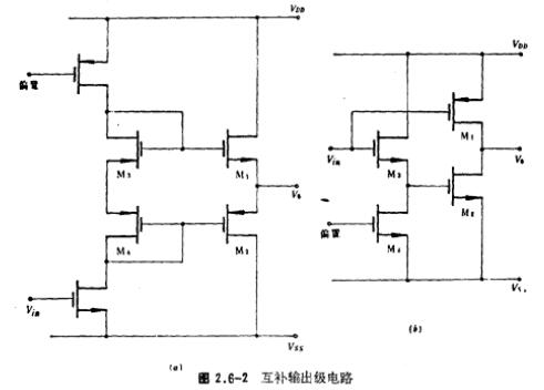
CMOS devices can be used to form complementary output stages similar to bipolar circuits, as shown in Figure 2.6-20, where M1 and M2 form complementary output stages, and M3 and M4 are their bias circuits. But as mentioned above, the output resistance of this circuit is relatively large, and its output voltage swing is not large enough. The output voltage swing of the circuit is not simply equal to the positive and negative power supply voltage minus the threshold voltage of each MOS tube. Due to the substrate bias effect, the threshold voltage of the output tube
As the output voltage increases, the output swing will decrease significantly. In order to achieve the largest possible output amplitude, the common source output stage circuit (not a follower) in Figure 2.6-26 can be used. Here M3 is the source follower, and its bias voltage also determines the quiescent current of M1 and M2. The bias voltage of M1 and M2 can be selected appropriately to make their quiescent working current very low and in a Class B executive state. At this time, when the input voltage changes in the positive direction, the current of M1 increases, and its source voltage also changes in the positive direction. CMOS complementary output stage. Therefore, the current of M2 increases, and the output voltage changes in the negative direction. At the same time, the current of M1 decreases, so the load current is provided by M2. Conversely, when the input voltage changes in the negative direction, the currents of M3 and M2 both decrease, and the output voltage changes in the positive direction. At the same time, the current of M1 increases, and it supplies current to the load. This kind of output circuit can be regarded as a kind of transconductance amplifier, when the load resistance is connected, it has a certain voltage gain. The circuit can output large positive and negative voltage swings (the positive and negative swings are determined by the positive and negative power supply voltage and the saturation voltage drop of M1 and M2), but its output resistance is very large, so it It is suitable for driving the internal nodes of MOS circuits.
For further discussion of the output stage circuit, please refer to the catalog article.

Contact: Mr. Zou
Contact number: 0755-83888366-8022
Mobile phone: 18123972950
QQ: 2880195519
Contact Address: 5C1, Block CD, Tianji Building, Tianan Digital City, Chegongmiao, Futian District, Shenzhen
Please search WeChat official account: "KIA Semiconductor" or scan the following picture to "Follow" official WeChat official account
Please "follow" the official WeChat account: provide MOS tube technical assistance


