Electronic Technology Forum
CMOS differential amplifier
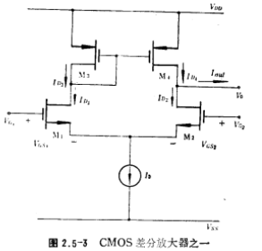
Figure 2.5-3 is a CMOS differential amplifier. N-channel MOS field effect transistors M1 and M2 are used as differential pairs, and its load is composed of P-channel current sources M3 and M4. The current source Io provides the work of the differential amplifier current.If M3 and M4 are matched, the currents of M3 and M4 are the same, that is
 , And the currents of M1 and M2 are also the same, so there is
 ,when
,when When the current of M1 and M2 are equal,
 ,make
,make ,Output current
 ;make
;make ,
,
 ,make
,make ,Output current
 ; Similarly, when
 ,
, ,because
 ,so
,so the increase is equal to
 the amount of reduction, and vice versa. Output current like this
 equal to the differential tube current
 the maximum value of the difference is the current Io, which realizes the conversion of the differential output signal of the differential amplifier into a single-ended output signal.

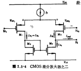
Figure 2.5-4 shows another form of CMOS differential amplifier. P-channel MOS transistors M1 and M2 are used as differential pairs, and N-channel MOS transistors M3 and M4 form a current source circuit as the load of the differential amplifier. The working current of the differential amplifier is provided by the current source IO. Obviously, the working principle of this circuit is the same as the circuit in Figure 2.5-3, but the substrate effect is different. If the CMOS process uses an N-type substrate, then the substrate of the P-channel MOS tube must be connected to the most positive potential of the circuit. (VDD), however, the substrate of the N-channel MOS tube is not necessarily connected to the most negative potential (Vss) of the circuit. The method is that the N-channel MOS tube is built on a separately formed P-well, so that the P-well is the same as the source of the MOS tube. The poles are connected, which eliminates the substrate termination effect. M; and M2 in Figure 2.5-3 are constructed in this way. Therefore, the CMOS differential amplifier of the N-channel MOS tube as a differential pair tube (Figure 2.5-3) has no substrate bias effect, while the CMOS differential amplifier of the P-channel MOS tube differential pair tube (Figure 2.5-4) has a substrate bias. effect.
The main performance of Fig. 2.5-4 CMOS differential amplifier is discussed below.

1. Voltage gain of CMOS differential amplifier
By (2.5-8) formula, the equivalent transconductance of the amplifier

Io is the operating current of the differential amplifier
 . Under equilibrium conditions, the output resistance of M₂ and M4
 respectively


So the voltage gain of the amplifier is

Where VO is the output voltage of the differential amplifier, and image.png is the differential mode input voltage of the differential amplifier. Substituting formulas (2.5-8) and (2.5-18~20) into the above formula, we get

This formula shows that the CMOS differential amplifier has a higher gain, and its gain is inversely proportional to the square root of the operating current ID, and the relationship curve between the gain and the operating current IO is similar to Figure 2.4-7.
2. Offset voltage of CMOS differential amplifier
For the circuit in Figure 2.5-3 (or Figure 2.5-4), its input offset voltage Vos should be composed of two parts: one is the influence of the mismatch of the input differential pair transistors M1 and M2, and the other is the active load M3 , The influence of M4 mismatch.
The input offset voltage caused by the mismatch of M1 and M2 is recorded as ,It is expressed by (2.5-14) formula, using (2.5-8) formula, we can get

where , Is the threshold voltage difference of M1 and M2,
 are the transconductances of M1 and M2, Δβ1 and β1 are the parameters of M1 and M2 respectively
 the difference and average value.
The input offset voltage caused by the M3 and M4 current source pair tube mismatch is recorded as , It is due to the mismatch of their current caused by the offset voltage of M3 and M4 to the tube itself, that is
 ,This current error causes M1 and M2 to produce the same current error for the tube, and the additional voltage generated by the offset voltage at the input is
 ,so
,so  it has the following relationship with the offset voltage of M3 and M4:

where transconductance of M3 and M4
 is the offset voltage of M3M4, it should also be determined by the formula (2.5-14), namely

Above is the difference in threshold voltage of M3 and M4, Δβ1 and β1 are the difference and average value of the parameters β of M3 and M4 respectively, namely

Substitute equation (2.5-24) into equation (2.5-23), for
for

The total offset voltage Vos is

Use (2.5-15) formula

The above formula shows that in order to reduce the input offset voltage of the differential amplifier, the difference between the threshold voltages of each pair of tubes should be reduced, and the width and length of the channel should be increased. Secondly, in order to reduce the mismatched input offset of M3 and M4 The influence of voltage, the ratio should be reduced , That is, reduce the ratio of the channel width to length ratio of M3 and M4 to the channel width to length ratio of M1 and M2
 therefore, the channel width-to-length ratio of M3 and M4 should be appropriately reduced during layout design, and the channel width-to-length ratio of M1 and M2 should be increased.
3. Noise of CMOS differential amplifier
The noise of the MOS tube is larger than that of the bipolar transistor, especially at low frequencies, there is a larger 1/f noise, so when designing the MOS amplifier, the noise of the amplifier should be considered. The noise mainly comes from the input stage of the amplifier, and in the MOS operational amplifier, a differential amplifier is used as the input stage. This section discusses the noise performance of CMOS differential amplifiers and how to reduce noise.
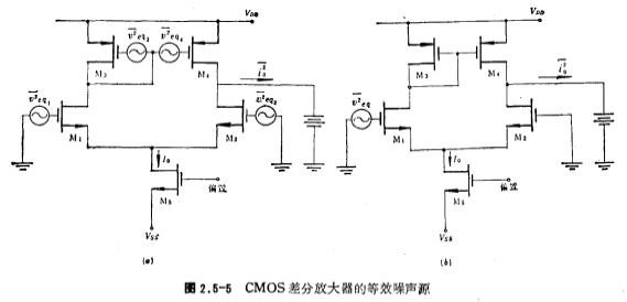
The equivalent noise source of the CMOS differential amplifier can be shown in Figure 2.5-5a. 以及
以及
They are respectively the mean square value of the noise voltage at the input terminals of M1, M2, M3 and M4.
For simplicity, consider the noise when the output is shorted. It can be seen from the figure that the mean square value of the total noise current given by the short circuit of the circuit is

Where is the transconductance of M1 and M2,
 it is the transconductance of M3 and M4.
If each noise source is equivalent to the input terminal, then Figure 2.5-5a can be drawn as Figure 2.5-5b. The mean square value of the total noise current output by the short circuit of the circuit should be

The output noise currents in these two equivalent circuits should be equal, so there is

It can be seen from the above formula that the noise of M1 and M2 is directly provided to the input of the amplifier, while the noise of M3 and M4 has the same effect on the input of the amplifier. Directly proportional. In order to reduce the influence of the noise of M3 and M4 on the amplifier, the transconductance value of M3 and M4 should be minimized in the circuit design.
 。
。

(2.5-30) Equivalent input noise in the formula it can be divided into 1/f noise and thermal noise, which are described as follows.
From the discussion in Chapter 1, we can see that the 1/f noise of the MOS tube is expressed as

Where KF is the 1/f noise figure.
The 1/1/f noise equivalent to the input end of the (2.5-30) and (1.3-42) CMOS integral division amplifiers can be expressed as (see reference [3])

where they are the 1/f noise figure of N-channel and P-channel MOS transistors, which are closely related to process conditions. It can be seen from the above formula that to reduce the 1/f noise of the differential amplifier, the channel area of the input pair M1 and M2 should be increased first
 , Secondly, make the active load to the channel length of tube M3, M4
 the channel length L1 is greater than M1 and M2.
The thermal noise of the MOS tube equivalent to the input is

By (2.5-30) and (2.5-32), the thermal noise equivalent to the input of the CMOS differential amplifier can be expressed as (see reference [3])

It can be seen from this formula that to reduce the thermal noise of the differential amplifier, the transconductance of the input pair M1 and M2 should be increased first, that is, increase the working current Io and increase the channel width-to-length ratio W1/L1, and then reduce Active load to the channel width-to-length ratio of M3 and M4 ,make
,make 。
。
4. Common mode rejection ratio (CMRR) of CMOS differential amplifier
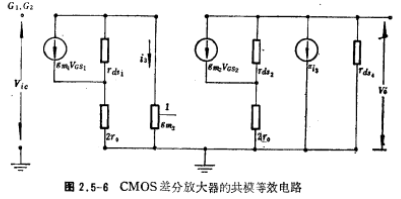
In the common mode signal Under the action, the equivalent circuit of Figure 2.5-3 is shown in Figure 2.5-6. In the figure, ro is the current source output interference,
 is the equivalent impedance of M2, a is the conversion coefficient of the current sources of M3 and M4. When M3 and M4 match, a=1. When M3 and M4 are mismatched, set a=1-Δa, and Δa is the mismatch error. Assume that the transconductance and output impedance of M1 and M2 are the same, that is
 。
。

From Figure 2.5-6, the common mode gain Ac can be solved as

By (2.5-20) formula, the differential gain of the differential amplifier is

For simplicity, we set here
According to the definition of common-mode rejection ratio, the CMRR of a CMOS differential amplifier is

It can be seen that to improve the common-mode rejection ratio of the differential amplifier, a high-impedance current source circuit should be selected to increase ro, and at the same time, the mismatch error Δa of the M3 and M4 tubes should be reduced.
The above discussion also applies to the Figure 2.5-4 CMOS differential amplifier.
Contact: Mr. Zou
Contact number: 0755-83888366-8022
Mobile phone: 18123972950
QQ: 2880195519
Contact Address: 5C1, Block CD, Tianji Building, Tianan Digital City, Chegongmiao, Futian District, Shenzhen
Please search WeChat official account: "KIA Semiconductor" or scan the following picture to "Follow" official WeChat official account
Please "follow" the official WeChat account: provide MOS tube technical assistance


