Electronic Technology Forum
Analysis of characteristic curve circuit of CMOS single-stage amplifier
Figure 2.4-1c, dCMOS single-stage amplifier, compared with Figure 2.4-1a, bNMOS single-stage amplifier, has a higher voltage gain and lower power consumption, the gain is generally up to 500~1000, based on its advantages, nearly a few In recent years, CMOS analog integrated circuits have made great progress.
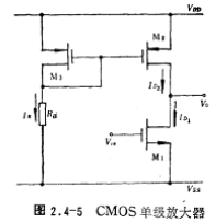
In the CMOS single-stage amplifier shown in Figure 2.4-1c, the active load M2 tube usually forms a current source circuit with the bias circuit, and the M2 tube acts as an active load. The circuit form is shown in Figure 2.4-5. For simplicity, assume that the channel width-to-length ratio of M1 and M2 are equal.

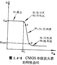
Input voltage When it is lower than the threshold voltage VT1 of the M1 tube, the M1 tube is turned off and the M2 tube is turned on, but there is no current, and the output voltage VO is equal to the power supply voltage VDD. When the input voltage
 when it is greater than VT1, M1 tube starts to conduct, and follow
 Increase, the output voltage VO decreases, when the current through the M1 and M2 tubes is equal to the reference current IR, the M2 tube enters the saturation region from the linear region. When the M1 and M2 tubes are both working in the saturation region, they will vary with the input voltage
 the increase of, the output voltage VO drops rapidly. When the input voltage
 when it increases to VO+VT1, the M1 tube enters the linear region from the saturation region. Figure 2.-5 The output voltage of the CMOS single-stage amplifier VO drops to the saturation voltage drop of the M1 tube
 figure 2.4-6 shows the input-output transmission characteristics of this circuit.

It can be seen from the figure that when the M1 and M2 tubes work in the saturation zone, the slope of the curve is the largest (section AB), and the small-signal gain of the AC is also the largest. It can be seen from the AC small signal equivalent circuit that the voltage gain of the M1 and M3 tubes working in the saturation region is equal to the product of the transconductance gm1 of the M1 tube and the output impedance of the M1 and M2 tubes in parallel, namely

Where


will ,substituting the expression into (2.4-14) to get

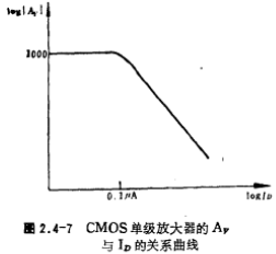
In the formula (2.4-15), we noticed an interesting conclusion, the working current ID decreases, the voltage gain AV increases, and AV can reach 500~2000, which is due to the output impedance of M1 and M2 It is inversely proportional to ID, while the transconductance gm1 is only proportional to the square root of 1D. Therefore, the difference between MOS circuit and bipolar circuit design is that the drain current of CMOS active load amplifier is smaller, and its voltage gain is higher. . Only when the current is reduced to make the MOS tube in the sub-threshold region, the transconductance of the FET will be proportional to the drain current. At this time, the voltage gain of the CMOS amplifier has nothing to do with the change of the operating current. For the CMOS amplifier shown in Figure 2.4-5, the relationship curve of IOgAv-IOgID is shown in Figure 2.4-7.
In addition, it can also be seen from the formula (2,-15) that the voltage gain is related to the modulation effect of the channel length. Obviously, increasing the channel length L can reduce the λ value and increase the output impedance of the MOS tube, thereby increasing the voltage gain. To further increase the voltage gain.
The M2 tube uses the high-impedance current source circuit described in the second section.
For the CMOS common-source amplifier circuit shown in Figure 2.4-1c, M2 can also be used as a common-source amplifier, and M1 can be used as an active load for M2.
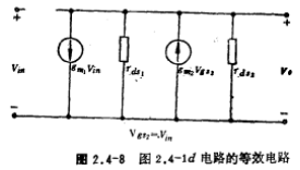
Figure 2.4-1d is a push-pull CMOS single-stage amplifier. The connection method of the circuit is different from that of Figure 2.4-1c, but the transmission characteristics of the circuit are the same. Here, some explanations will be made on the small-signal voltage gain of the circuit. When both M1 and M2 of the circuit in Figure 2.4-1d work in the saturation region, the AC small-signal equivalent circuit diagram is shown in 2.4-8.


In the picture the small signal voltage gain is

where

The above formula shows that the push-pull CMOS single-stage amplifier has a larger gain, which can reach 500~2000. The voltage gain Av is also inversely proportional to the square root of the operating current ID.
Relevant information
Contact: Mr. Zou
Contact number: 0755-83888366-8022
Mobile phone: 18123972950
QQ: 2880195519
Contact Address: 5C1, Block CD, Tianji Building, Tianan Digital City, Chegongmiao, Futian District, Shenzhen
Please search WeChat official account: "KIA Semiconductor" or scan the following picture to "Follow" official WeChat official account
Please "follow" the official WeChat account: provide MOS tube technical assistance


