Electronic Technology Forum
Detailed analysis of the working status of NMOS single-stage amplifier
1. Fully enhanced NMOS amplifier (Figure 2.4-1a)
(1) Input-output transmission characteristic curve of the amplifier
The amplifier has three working states:
i. Input voltage of M1 tube less than the turn-on voltage
 ,scilicet
 the tubes are all cut off, and the output voltage VO is high. When the M2 tube is cut off, there is, The output voltage VO value is in the range of VDD-VT1<VO<VDD.
ii. When ,The M1 tube enters the saturation zone from the cut-off zone, and the ID1 current of the M1 tube follows
 at the same time, the M2 tube also enters the saturation region from the cut-off region. Because the M2 tube and M●1 tube are connected in series, the drain-source current is the same, that is, ID1=ID2, so ID2 also follows
 the increase of ID2 is due to the increase of VGS. In this way, the current is gradually increased from cut-off to conduction, and the output voltage VO starts to decrease slowly from VO=VDD-VT1. If the output voltage VO is greater than
 ,The M1 tube is in the saturation zone. Once the M2 tube is turned on, it is always in the saturation zone.
iii. When ,the M1 tube enters the linear region from the saturation region, the output voltage VO further drops, and the falling speed slows down.
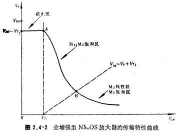
Based on the above discussion, the input-output transmission characteristic curve of the amplifier can be drawn. The curve is shown in Figure 2.4-2.
It can be seen from Figure 2.4-2 that the boundary between the cut-off zone and the saturation zone is the straight line.the AB section of the curve is the saturation region, the slope of which is the largest in the transmission characteristic curve. Therefore, the amplifier must obtain a higher gain, and the M1 and M2 tubes should work in the saturation region. Properly biasing the DC voltage on the gate of the M1 tube can make the amplifier enter the saturation region.
(2) AC small signal gain
When both M1 and M2 tubes work in the saturation zone, the following equation can be obtained

Since ID1=ID2, it can be obtained by (2.4-1) and (2.4-2)

From the above formula, the AC small signal gain of the amplifier in Figure 2.4-1a can be obtained, which is expressed as

It can also be obtained directly from the AC small signal equivalent circuit. The small signal equivalent circuit is shown in Figure 2.4-3.AC small signal gain
Obtained from Figure 2.4-3For Figure 2.4-1a, in Figure 2.4-3
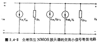
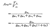
where .If the output impedance of the M1 and M2 tubes is ignored, the above formula can be written as

According to the definition of η (see Chapter 1, Section 3), (2.4-6) and (2.4-4) are the same.
It can be seen from the formula (2.4-4) or (2.4-6) that to increase the amplifier gain AVE in Figure 2.4-1a, the only way to increase the channel width-to-length ratio W1/L1 of the M1 tube and reduce the channel width and length of the M2 tube Ratio W2/L2, make W1/L1>W2/L2; if W1/L1=1000W2/L2, regardless of the substrate bias effect of the M2 tube, then the maximum gain is only 10 times. Therefore, the gain of the fully enhanced NMOS single-stage amplifier in Figure 2.4-1a is relatively low, usually only a few times.
Let us explain the reason for the low AVE from another aspect. According to the analysis in the first section of this chapter, the equivalent load ro of the M2 tube is equal to 1/gm, usually 1/gm is small, so the gain AVE is not large. To increase the gain, the depletion type E/D MOS amplifier shown in Figure 2.4-1b can be used as the load.
2. E/D MOS single-stage amplifier (Figure 2.4-1b)
In order to improve the voltage gain of the NMOS amplifier, the n-channel enhancement mode MOS tube M2, which is shown in Figure 2.4-1a as the equivalent load, is replaced by an n-channel depletion mode MOS tube.
(1) Input-output transmission characteristic curve
i、 ,the M1 tube is in an off state, and the output voltage Vo=VDD.
ii、 ,the M1 and M2 tubes are turned on. The M1 tube works in the saturation zone. The M2 tube is in the linear region when the M1 tube is just turned on because the output voltage Vo is relatively large.
 增大,电流ID增大,输出电压Vo降至Vo<VDD+VT1时,M2管进入饱和区。由图2.4-1b可知,M2管进入饱和区后,
  Increase slightly to make
 Increase rapidly, so that the output voltage Vo drops rapidly.
iii、 when the M1 tube enters the linear region from the saturation zone, the M₂ tube is still in the saturation zone, and the output voltage Vo drops slowly.
In summary, the input-output characteristic curve of Figure 2.4-1b is shown in Figure 2.4.4.
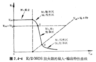
It can be seen from the figure that the slope of the AB section of the curve is the largest, and its AC small signal gain is also the largest. Therefore, when Figure 2.4-1b is used for small signal amplification, both M1 and M₂ tubes should work in the saturation zone.
(2) AC small signal gain
When both M1 and M₂ tubes work in the saturation zone, the following relationship can be obtained:
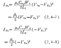
because ,By (2.4-7), (2.4-8) formula

From the above formula, the gain AVD of the E/D NMOS line amplifier is

AVD can also be obtained by AC small signal equivalent circuit diagram 2.4-3

Regardless of the output impedance of the M1 and M2 tubes, the above formula is written as

The formula (2.4-12) is the same as the formula (2.4-10). Comparing (2.4-12) formula and (2.4-6) formula, AVD and AVE have the following relational formula, namely

Since η2 is approximately equal to about 0.1, AVD is one order of magnitude larger than AVE. Therefore, the gain of an amplifier with a depletion type as a load is greater than that of an amplifier with an enhanced type as a load. Therefore, E/D is often used in NMOS amplifier circuits. MOS circuit to improve voltage gain.
According to (2.4-10) formula or (2.4-12) formula, increase the AVE gain, the M1 tube transconductance bigger, M2 tube transconductance
 To be small, i.e.
 The ratio is greater. Although the voltage gain AVD of the E/DMOS single-stage amplifier is larger than the voltage gain AVE of the fully enhanced NMOS single-stage amplifier, it is only a few dozen times or so.
Contact: Mr. Zou
Contact number: 0755-83888366-8022
Mobile phone: 18123972950
QQ: 2880195519
Contact Address: 5C1, Block CD, Tianji Building, Tianan Digital City, Chegongmiao, Futian District, Shenzhen
Please search WeChat official account: "KIA Semiconductor" or scan the following picture to "Follow" official WeChat official account
Please "follow" the official WeChat account: provide MOS tube technical assistance


