Electronic Technology Forum
Analysis and Analysis of CMOS Tube Bias Circuit
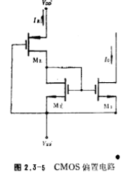
The so-called CMOS bias circuit is to combine the bias resistor in Figure 2.3-1 ,Use a P-channel MOS tube instead. The circuit form is shown in Figure 2.3-5. In 1CMOS operational amplifiers and other MOS analog circuits, the bias circuit generally adopts the circuit form of Figure 2.3-5.

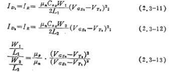
The design formula is as follows:

In the formula it is the hole mobility in the p-channel, and is usually 1/2 to 1/4 of the electron mobility μn in the n-channel.

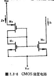
In the low power supply voltage, low power consumption CMOS operational amplifier circuit, the bias circuit sometimes adopts the circuit form of Figure 2.3-6. At this time, the M2 tube works in the linear region. And have a larger Therefore, the channel width and length of the M2 tube are relatively small. Computer analysis shows that the bias stability of the circuit in Figure 2.3-6 is better than that in Figure 2.3-6. The design formula is
Contact: Mr. Zou
Contact number: 0755-83888366-8022
Mobile phone: 18123972950
QQ: 2880195519
Contact Address: 5C1, Block CD, Tianji Building, Tianan Digital City, Chegongmiao, Futian District, Shenzhen
Please search WeChat official account: "KIA Semiconductor" or scan the following picture to "Follow" official WeChat official account
Please "follow" the official WeChat account: provide MOS tube technical assistance


