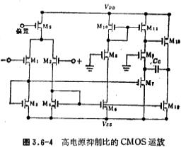
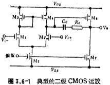
CMOS improves the power supply rejection ratio. The reason why the power supply rejection ratio of the op amp circuit shown in Figure 3.6-1 is relatively poor is mainly caused by the coupling of the s
CMOS improves the power supply rejection ratio. The reason why the power supply rejection ratio of the op amp circuit shown in Figure 3.6-1 is relatively poor is mainly caused by the coupling of the s
CMOS op amp power supply rejection ratio, MOS large-scale integrated circuits have both analog and digital circuits, that is, the analog circuit and the digital circuit are built on the same chip, so
CMOS op amp power supply rejection ratio, MOS large-scale integrated circuits have both analog and digital circuits, that is, the analog circuit and the digital circuit are built on the same chip, so
CMOS operational amplifier current conversion type, high-speed CMOS operational amplifier current conversion type parameters and amplifier stage circuit detailed explanation 1. The block diagram of th
CMOS operational amplifier current conversion type, high-speed CMOS operational amplifier current conversion type parameters and amplifier stage circuit detailed explanation 1. The block diagram of th
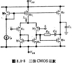
In many practical applications, such as high-speed A/D, D/A converters and high-frequency switched capacitor filters, op amps are required to have a higher frequency settling time.
In many practical applications, such as high-speed A/D, D/A converters and high-frequency switched capacitor filters, op amps are required to have a higher frequency settling time.
CMOS operational amplifier circuit diagrams, most of the introductions are CMOS operational amplifiers used in LSI MOS analog integrated circuits. Figure 3.4-10 is the circuit diagram of the monolithi
CMOS operational amplifier circuit diagrams, most of the introductions are CMOS operational amplifiers used in LSI MOS analog integrated circuits. Figure 3.4-10 is the circuit diagram of the monolithi
Low-voltage, low-power CMOS operational amplifiers, low-power operational amplifiers, low-voltage, low-power CMOS operational amplifiers are not difficult to design, it is not much different from gene
Low-voltage, low-power CMOS operational amplifiers, low-power operational amplifiers, low-voltage, low-power CMOS operational amplifiers are not difficult to design, it is not much different from gene
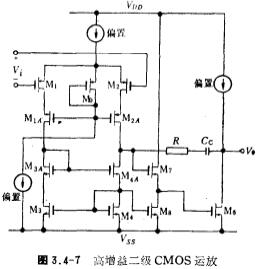
High-gain CMOS, in order to increase the gain, the load of the input stage (differential amplifier) adopts the high-impedance current source circuit M3∧, M4∧, M3 and M4 introduced in the second secti
High-gain CMOS, in order to increase the gain, the load of the input stage (differential amplifier) adopts the high-impedance current source circuit M3∧, M4∧, M3 and M4 introduced in the second secti
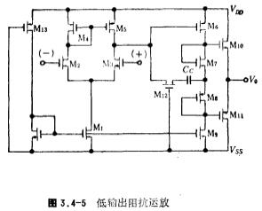
CMOS output impedance, Figure 3.4-5 is a low output impedance op amp. The output stage adopts Class A and Class B push-pull amplifiers, which can drive a low resistance load of 200 ohms. In order to r
CMOS output impedance, Figure 3.4-5 is a low output impedance op amp. The output stage adopts Class A and Class B push-pull amplifiers, which can drive a low resistance load of 200 ohms. In order to r

The working principle of CMOS operational amplifier circuit, the potential of node ⑦ in the circuit is determined according to the maximum amplitude of the forward voltage output by the circuit, the o
The working principle of CMOS operational amplifier circuit, the potential of node ⑦ in the circuit is determined according to the maximum amplitude of the forward voltage output by the circuit, the o
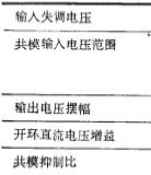
CMOS setup time, CMOS conversion time, and the frequency characteristics of CMOS op amps refer to the rate response when working in small signals. They are usually described by small signals (sine sig
CMOS setup time, CMOS conversion time, and the frequency characteristics of CMOS op amps refer to the rate response when working in small signals. They are usually described by small signals (sine sig


5C1, CD Block, Tianji Building, Tianan Digital City, Futian District, Shenzhen

KIA-The Public