Electronic Technology Forum
Detailed explanation of high-speed CMOS operational amplifier current conversion parameters and amplifier stage circuit
1. Block diagram and basic relational expression of current conversion op amp
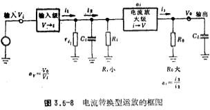
The block diagram of the current conversion op amp is shown in Figure 3.5-8. The input stage converts the input voltage into current, and this current is amplified by the current amplifier stage and sent to the output terminal. is the output impedance of the input stage,
 is the input impedance of the current amplifier stage,
 is the equivalent input capacitance of the current amplifier stage,
 is the output impedance of the current amplifier stage, and CL is the load capacitance. To improve the voltage gain and unity gain bandwidth of the amplifier. CMOS operational amplifier current conversion type. Usually use low input impedance
 、Low input capacitance
 、High output impedance
 and the current amplifier circuit with high current gain. The equivalent circuit of Figure 3.5-8 is shown in Figure 3.5-9.
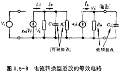
consider ,from Figure 3.5-9, the low-frequency pole frequency of the amplifier can be obtained as

The high frequency pole frequency is

The low frequency voltage gain is

where Is the magnification of the current amplifier stage.
Usually the high pole frequency shown in equation (3.5-6) is higher than the unity gain bandwidth frequency GB, so the unity gain bandwidth frequency GB can be written as

According to the discussion in the first section of this chapter, the op-amp can work stably under deep negative feedback. The minimum value of the high-frequency pole frequency ω2 should be equal to the unity gain bandwidth frequency GB, which is defined by (3.5-6) and (3.5-8) , We can find the minimum load capacitance (that is, compensation capacitance).

2. Current amplifier stage circuit
The current amplifier stage circuit is realized by the current source circuit, and its basic current amplifier stage circuit is shown in Figure 3.5-10.
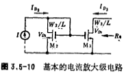
According to the discussion in Section 2 of Chapter 2, the main parameters of the circuit shown in Figure 3.5-10 are:
Output impedance

input resistance

Current gain

In order to obtain a higher unity gain bandwidth frequency, the channel lengths of M2 and M3 are smaller, so. The channel length modulation effect cannot be ignored, and the output impedance Ro is small. In order to increase the output impedance, the cascade form of high-impedance current source introduced in Section 2 of Chapter 2 can be used as the current amplifying stage circuit. The circuit form is shown in Figure 3.5-11.
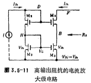
The output impedance of the circuit shown in Figure 3.5-11 (refer to Chapter 2 Section 2 (2.2-4) Equation

input resistance

Current gain large-scale circuit

The cascade high resistance current source is used as the current conversion operational amplifier of the current amplifier. The equivalent schematic diagram is shown in Figure 3.5-12.
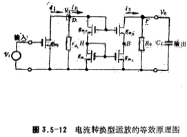
From Figure 3.5-12 and (3.5-10), (3.5-13~15) equations, the gain of the amplifier can be obtained as

It can be seen that in a given under the condition of increasing
 transconductance
 , Can improve the voltage gain of the current conversion op amp.
3. The actual circuit of the current conversion type high-speed CMOS operational amplifier
The actual circuit diagram of the current conversion type high-speed CMOS operational amplifier is shown in Figure 3.5-13. The input stage circuit is composed of , Constitute a differential amplifier, which converts the input signal voltage into current;
 It forms a current amplifier stage circuit with high output impedance, which amplifies the current of the input stage and delivers it to the output end; CMOS operational amplifier current conversion type.
 a high-impedance current source is formed, which converts the double-ended output current into a single-ended output, so that the double-ended input is amplified and then the single-ended output is realized. CL is the load capacitance and also used as the rate compensation capacitance. The minimum value of CL is determined by the formula (3.5-9). The conversion rate of this circuit is determined by the following formula:

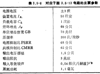
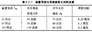
In order to obtain a higher unity gain bandwidth GB and slew rate SR, the device in Figure 3.5-13 uses a short-channel MOS tube with L=1.5 microns. The main parameters of the circuit are shown in Table 3.5-6, where VDD= Under the condition of ±3V, Vcc=-3V, CL=1 picofarad, the relationship between the size of the bias current  and the main parameters of the circuit is listed in Table 3.5-7.
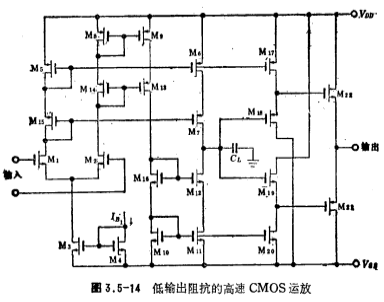
in order to obtain a low output impedance, an output stage circuit is added on the basis of Figure 3.5-13. The circuit form is shown in Figure 3.5-14. M17~M21 form a low output impedance output stage circuit, and its preamplifier part is connected with The circuit in Figure 3.5-13 is the same. Compared with the circuit in Figure 3.5-13, this circuit reduces the output impedance, but the output swing is reduced.
Contact: Mr. Zou
Contact number: 0755-83888366-8022
Mobile phone: 18123972950
QQ: 2880195519
Contact Address: 5C1, Block CD, Tianji Building, Tianan Digital City, Chegongmiao, Futian District, Shenzhen
Please search WeChat official account: "KIA Semiconductor" or scan the following picture to "Follow" official WeChat official account
Please "follow" the official WeChat account: provide MOS tube technical assistance


