Electronic Technology Forum
Monolithic CMOS operational amplifier bias and input stage and output stage design circuit diagram
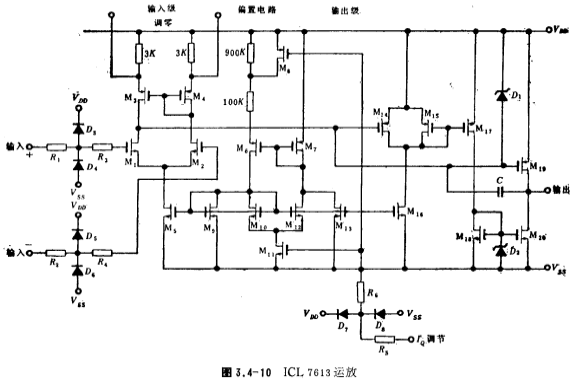
Most of the above are CMOS operational amplifiers used in LSI MOS analog integrated circuits. Figure 3.4-10 is the circuit diagram of the monolithic CMOS operational amplifier ICL7613. CMOS operational amplifier circuit diagram. Its power consumption current can be adjusted externally, the minimum power consumption current is 10 microamperes, and the lowest power supply voltage that can be used is ±0.5 volts, so it is a micro-power operational amplifier.
The ICL7613 circuit is composed of three parts, namely the input stage, the output stage and the bias circuit.

1. CMOS input stage
The input stage of the circuit is a differential amplifier stage composed of n-channel MOS transistors M1 and M2, and P-channel MOS transistors M3 and M4 are its active loads, and at the same time it realizes a double-ended-single-ended conversion function. The sources of M3 and M4 are connected with resistors to increase the equivalent output resistance of M3 and M4 and realize zero offset adjustment.
2. CMOS bias circuit
The bias circuit of the op amp is composed of p-channel MOS tube . And n-channel MOS tube
 composition. The source of M6 is connected to a large resistance, so its current will be much smaller than that of the M7 tube. The current of M6 is used to bias the input stage circuit, and the current of M7 is used to bias the output stage circuit. 70% of the bias current of the entire circuit is supplied to the output stage. Therefore, the current of M7 is larger than that of M6. CMOS operational amplifier circuit diagram.
 the current is given by
 the current source circuit of M7 is provided to the input stage, and the current of M7 is biased by M13 to M10, M10 and M12 and acts as a shunt to achieve the purpose of bias current adjustment. When the bias current IQ adjustment terminal is connected to the positive power supply,
 Cut off, the current of M6 is very small. At the same time, the current of M11 is larger, that is, the currents of M10 and M12 are larger, so that the currents of M9 and M10 are reduced, which reduces the currents of the input and output stages. In the circuit design, the total current at this time is about 10 microamperes. When the bias current IQ adjustment terminal is connected to a negative current, the current of M9 is larger, and M11 is cut off. M10 and M12 do not have the function of shunting. Therefore, the input and output stage currents increase, and the positive current of the circuit is about 1 mA. When the bias current IQ adjusting terminal is grounded, the current is between the above two situations, and the total current of the circuit at this time is about 100 microamperes.
3. CMOS output stage
The output stage circuit is composed of M14~M20. M19 and M20 constitute a common source output stage, and its drive circuit form is briefly introduced here. The current of M10 in the circuit is biased by M7 and M13 meters. When the gate voltage of M14 increases, its current decreases, so the current supplied by M16 to M15 increases. Since M15 and M17 form a current source, the current of M17 increases accordingly. Through the function of the current source of M18 and M20, the current of M20 is increased. At the same time, since the gates of M10 and M14 are connected at the same point, the current of M19 also drops. At this time, the output voltage of the circuit changes to the negative direction, and its load current will be mainly provided by M20. CMOS operational amplifier circuit diagram. Conversely, when the gate voltage of M14 decreases,
The gate voltage of the SR also decreases, and the output voltage changes in the positive direction. At this time, the current of M14 increases, the current of M15 decreases, and the current of M20 eventually decreases. Therefore, the load current of this land will be provided by M10. Obviously, the output stage is also a voltage gain stage. The capacitor C in the output stage is a must-rate compensation capacitor. D1 and D2 are protection tubes of the output circuit.
When the external load resistance of the circuit becomes smaller, the forward voltage swing of the op amp will be limited by the positive power supply voltage, and the negative voltage swing will be limited by the bias current. Because the negative load current of the circuit is determined by M2. Provided, it cannot exceed the total current of the circuit. Therefore, when the load resistance becomes smaller, its negative output swing is limited by the bias current.
When the bias current of the op amp changes, the circuit parameters will change accordingly. When the bias current is small, the input noise voltage will decrease and the gain will increase slightly (the reason has been discussed in the previous chapter). At this time, the slew rate of the circuit will decrease. When the bias current increases to 1 mA, the conversion rate of the circuit increases accordingly.
In addition, the input terminal of the circuit is connected with a protection circuit, the resistance in Figure 3.4-10 and the diode
 it is set up for this purpose. CMOS operational amplifier circuit diagram. When the input sensing signal is greater than the positive and negative power supply voltages, the diode is turned on. Because of its clamping effect, the input voltage is limited within the range of positive and negative power supply voltages. resistance
 it is the high current resistance of the diode.
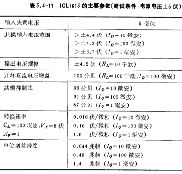
The main parameters of ICL7613 are shown in Table 3.4-11.

Contact: Mr. Zou
Contact number: 0755-83888366-8022
Mobile phone: 18123972950
QQ: 2880195519
Contact Address: 5C1, Block CD, Tianji Building, Tianan Digital City, Chegongmiao, Futian District, Shenzhen
Please search WeChat official account: "KIA Semiconductor" or scan the following picture to "Follow" official WeChat official account
Please "follow" the official WeChat account: provide MOS tube technical assistance


