Electronic Technology Forum
High-speed CMOS op amp cascode characteristics and circuit details
In many practical applications, such as high-speed A/D, D/A converters and high-frequency switched capacitor filters, op amps are required to have a higher frequency settling time. For example, for high-speed A/D and D/A converters, the settling time of the operational amplifier often determines the conversion speed of the A/D and D/A converters. It can be said that the shorter the settling time of the op amp, the faster its speed.
From the discussion in the third section of this chapter, it can be seen that the wider the unity gain bandwidth of the op amp and the higher the high-frequency pole frequency, the shorter the settling time. Therefore, the design of high-speed CMOS op amps mainly depends on how to increase the unity gain bandwidth and high-frequency poles. Rate. CMOS op amp common source-common gate. At present, high-speed CMOS operational amplifier circuits mainly have two forms: cascode circuit structure; current conversion circuit structure. Discuss these two kinds of high-speed CMOS operational amplifier circuits separately now.
The design of the usual CMOS operational amplifier mainly adopts the circuit form of two-stage amplification, and its simplified equivalent circuit diagram is shown in Figure 3.5-1. This circuit structure is relatively simple, and the design technology has become mature, but the pole caused by the internal compensation capacitor Cc determines that the unity gain bandwidth of the op amp cannot be very wide, usually about 1 to 2 MHz, which limits the speed of the op amp. The single-stage common-source common-shed CMOS op amp introduced in this section overcomes the shortcomings of the op amp in Figure 3.5-1, such as not wide unity gain bandwidth, and improves the speed of the op amp. Its simplified form is shown in Figure 3.5-2.
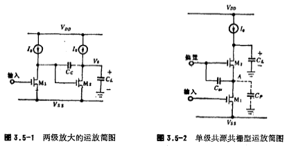
For simplicity, suppose the transconductance of the MOS device is gm, the output impedance is ro, and the load is an ideal current source. From Figure 3.5-1 and Figure 3.5-2, the low-frequency pole P1 and high-frequency pole P2 of the two-stage amplifier and single-stage cascode amplifier can be obtained respectively, and their values are listed in Table 3.5-1.

Obtained from Table 3.5-1.

Usually the distributed capacitance CT in Figure 3.5-2 is the load capacitance CL Therefore, the high-frequency pole P2 of the single-stage cascode amplifier is 5-10 times higher than that of the two-stage amplifier. CMOS op amp common source-common gate. Obviously, the settling time of an op amp composed of a single-stage cascode amplifier is shorter than that of an op amp composed of a two-stage amplifier. Figures 3.5-3a~c are simplified operational amplifier schematics, simplified diagrams and small-signal AC equivalent circuits composed of single-stage cascode amplifiers. Rs and RL in the figure represent the limited output impedance of the current source. From Figure C, the voltage gain is

where They are the transconductance and output impedance of NMOS and PMOS devices, Rs and RL are the finite current source
Rn is the equivalent impedance seen from the source of the P-channel device, and its value is

If the output impedance of the load is much larger than the output impedance of the MOS tube, then the maximum gain of the single-stage cascode op amp is

It can be seen from the above formula that the maximum gain is the same as the DC gain of the two-stage op amp.
1. The characteristics of cascode op amp with double-ended output
Compared with the commonly used two-stage amplifiers, the op amp shown in Figure 3.5-3 has the following characteristics:
(1) Due to the single-stage cascode amplifier circuit form, the circuit has a very high sub-pole frequency ω2, and the corresponding transient response set-up time TssT is relatively small;
(2) The load capacitor is also used as a compensation capacitor, thereby simply solving the frequency compensation problem and reducing the chip area;
(3) The bias circuit of this op amp is more complicated than the commonly used two-stage op amp.
2. Double-terminal output cascode op amp
In order to make the single-stage cascode op amp have a higher gain, the active load of the output stage can be used with the high-impedance current source in the second section of Chapter 2. The actual circuit of a single-stage cascode op amp is shown in Figure 3.5-4, which is a circuit form of double-ended input and double-ended output.
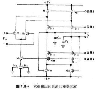
In the figure, M1~M2 are input stage differential amplifiers, M4~M9 constitute the output stage circuit, among which M6 and M7 are current sources, M8 and M9 are shared-house amplifiers; M10~M13 constitute the active load of the output stage; M14, M15 forms a common-mode negative feedback circuit. In order to eliminate the influence of the common-mode feedback circuit (M14, M15) on the operating point of the circuit, M4 and M5 tubes are connected to the source of M3, and their parameters are the same as those of M14 and M15. The working current of the circuit is provided by the bias circuit. Now give a brief description of the working principle and design method of the circuit in Figure 3.5-4. In the static bar, the working current of M1 and M2, M6 and M7 are the same. Part of the current of M6 and M7 flows into the differential amplifier M1 and M2 and the other part flows into the common gate circuit M8 and M9. To ensure zero input, the output voltage is also Zero, the working current of the active load M10~M13 should be the same as the current of M5 and M6. When the positive input signal acts on the input terminal M1, the current of M1 increases and the current of M2 decreases, because the current flowing through M6 and M7 remains unchanged. In this way, the current decreases, the current of M9 increases, and the active load is a constant current source circuit, and its current is constant. Therefore, the voltage obtained at the output terminal is
 current and
  the difference in current is proportional, and its polarity is positive. When a negative input signal acts on the input terminal M1, the voltage obtained at the output terminal is negative. Obviously, in order to obtain a higher voltage gain, the input stage transconductance should be increased, and the output impedance of the output stages M8 and M9 should be increased. And increase the output impedance of the active load. CMOS op amp common source-common gate. Because the current source is cascaded, in order to obtain a large output amplitude, the current source and bias circuit can adopt the circuit form shown in Figure 2.2-8 in Chapter 2. Now briefly introduce the role of common mode negative feedback circuits M14 and M15. When the terminal common mode level increases, the on-resistance of M14 and M15 decreases, and the current flowing through M10, M12 and M11, M13 increases, causing the output terminal level to decrease at the same time. On the contrary, make the output level rise. Therefore, the common mode feedback can stabilize the operating point without affecting the differential mode signal at the output.
3. The actual circuit of the double-ended output cascode op amp
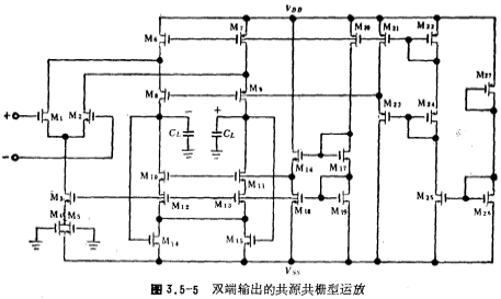
The actual circuit diagram of the cascode op amp including the bias circuit is shown in Figure 3.5-5.
In the figure, M1~M3 are input stage differential amplifiers (equivalent to common source amplifiers). In order to increase the gain of the input stage and reduce noise, the size of the input tube should be designed to be larger. M8 and M9 are common gate circuits; M6, M7 and M10~M13 respectively constitute current source circuits; M14 and M15 constitute common mode feedback circuits. In order to obtain a higher gain, the output stage current source adopts the constant current source circuit with high impedance and large output amplitude as shown in Figure 2.2-8 in the second section of Chapter 2. The n-channel high-impedance current source and bias circuit are composed of M10~M13 and constituted; p-channel high-impedance current source and bias circuit are composed of
 constituted. In the picture
 it is the total bias circuit.
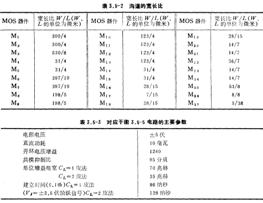
Considering speed requirements, power consumption and chip area, after design and computer simulation, the length ratio of each tube in the circuit in Figure 3.5-5 is shown in Table 3.5-2, and its main parameters are listed in Table 3.5-3.
4. Single-ended output cascode op amp circuit
Make some corresponding changes in the output circuit of Figure 3.5-5 to get a single-ended output cascode op amp circuit. The specific circuit is shown in Figure 3.5-6. use the current source circuit can convert double-ended output into single-ended output. The main parameters of the circuit and the aspect ratio of the device are listed in 3.5-4 and Table 3.5-5, respectively.
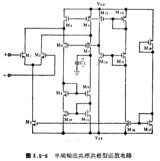
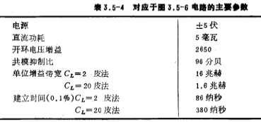

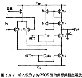
Figure 3.5-5 and Figure 3.5-6 cascode MOS operational amplifier, its input stage adopts n-channel MOS differential amplifier, if the input stage adopts p-channel MOS differential amplifier, the circuit form is shown in Figure 3.5-7.
Contact: Mr. Zou
Contact number: 0755-83888366-8022
Mobile phone: 18123972950
QQ: 2880195519
Contact Address: 5C1, Block CD, Tianji Building, Tianan Digital City, Chegongmiao, Futian District, Shenzhen
Please search WeChat official account: "KIA Semiconductor" or scan the following picture to "Follow" official WeChat official account
Please "follow" the official WeChat account: provide MOS tube technical assistance


